

One of the luckiest coincidences in the past decade has been that the hybrid machines designed for traditional HPC simulation and modeling workloads. which combine the serial processing performance of CPUs and the parallel processing and massive memory bandwidth of GPUs, were also well suited to run machine learning training applications.
If the HPC community had not made the investments in hybrid architectures, the hyperscalers and their massive machine learning operations, which drive just about all aspects of their businesses these days, would not have seen such stellar results. (And had that not happened, many of us would have had jobs for a bit longer some years hence, but that is a different story.)
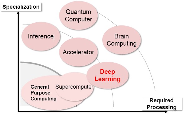
But not everyone believes that HPC iron and machine learning/deep learning iron will necessarily converge, and there are more than a few companies that are creating specialized processors to accelerate various ML/DL tasks – Nervana Systems (now part of Intel), Google, Graphcore, and Knupath are but some examples. But Japanese computing giant Fujitsu. Which knows a thing or two about making a very efficient and highly scalable system for HPC workloads, as evidenced by the K supercomputer, does not believe that the HPC and AI architectures will converge. Rather, the company is banking on the fact that these architectures will diverge and will require very specialized functions. And that is why Fujitsu is creating its own deep learning processor, which will come to market in its fiscal 2018 year, which ends next March.
If you want to be honest about it, Fujitsu actually believes in a divergence that covers four distinct markets:
- Legacy workloads in the enterprise running on proprietary GS mainframes
- Newer big iron enterprise workloads such as relational databases and their ERP stacks running on high-end NUMA Sparc64 systems
- Simulation and modeling workloads on PrimeHPC clusters with their unique interconnect and floating point processing demands
- Emerging and rapidly maturing deep learning applications running on future Deep Leaning Unit, or DLU, processors.
To get a feel for their similarities and longevity, take a look at this roadmap that covers the past several decades of processor development, which Takumi Maruyama, senior director of the AI Platform business of the Advanced System Research and Development unit at Fujitsu, presented at the International Supercomputing conference recently:
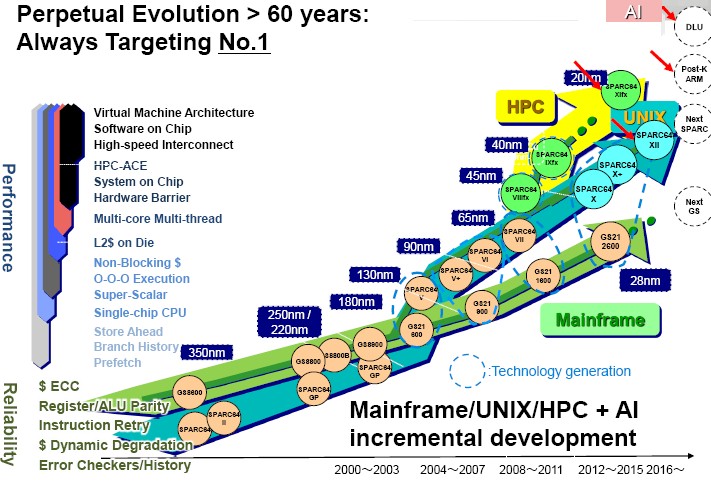
While we are knowledgeable about mainframes, and these systems were arguably the first platforms in the datacenter, only a few thousands companies worldwide are committed to proprietary mainframes and they are by no means mainstream even if they are important and, from our perspective, show how a system can evolve and stay relevant over decades. (There are lessons here.)
We have profiled the Sparc64-XII processor that is in development for Fujitsu’s Sparc64 NUMA machines, which at twelve cores have fewer but brawnier cores than its predecessor, the sixteen-core Sparc64-X+, which came out four years ago. The Sparc64-XII has eight threads each on those dozen cores, which are cranked up to 4.25 GHz with a turbo mode that reaches 4.35 GHz. The chip has 5.45 billion transistors and has 32 MB of L3 cache and embedded memory controllers (two DDR3) and I/O controllers (two PCI-Express 3.0), and its memory throughput is 153 GB/sec. (It would be interesting to see what this chip could do with DDR4 interfaces. But NUMA chips are wide, and slower DDR3 is cheaper in big gobs than faster DDR4. This chip can do 417 gigaops on integer math (yes, that is ugly, and it would be nice if this abbreviation was called giga-ips or something like that) and 835 gigaflops on its floating point units at double precision. This monster is etched using 20 nanometer processes from Taiwan Semiconductor Manufacturing Corp, which has been Fujitsu’s fab partner for the past several years.
The Sparc64-XIfx chip, which debuted in 2014 and which we detailed here, is aimed at HPC workloads and crammed 32 cores with special 256-bit HPC-ACE2 vector functions plus two helper cores onto a package with Hybrid Memory Cube (HMC) memory on the interposer. The Sparc64-XIfx chip has 3.75 billion transistors, a lot of which come from the 24 MB of L2 cache (the highest level it has). This chip runs at the single speed of 2.2 GHz delivers 1.1 teraflops of performance and has what Maruyama called medium-sized CPUs. That HMC memory delivered 480 GB/sec of bandwidth – about six times that of a “Haswell” or “Broadwell” Xeon processor and about eight times more than the 64 GB/sec of memory bandwidth into and out of the Sparc64-VIIIfx chip used in the K super, which delivered 128 gigaflops per socket. The Sparc64-XIfx represented nearly an order of magnitude in performance and memory bandwidth per socket, which is not bad.
Going forward, Fujitsu is working with the Japanese government and its RIKEN HPC center to develop a Post-K machine based on ARM processors with even more sophisticated vector extensions, and it is abandoning the Sparc instruction set for the HPC crowd in an effort to make something that is more mainstream. The goal with the Post-K exascale system is to deliver 100X the performance of the K supercomputer when gauged in peak theoretical performance and 50X on real-world applications that have been running on the K system – all within a thermal envelope of 30 megawatts to 40 megawatts. (That will probably creep up.)
The current Sparc64-XIfx processors were linked together with the Tofu2 interconnect, the follow-on to the original Tofu 6D mesh/torus interconnect used in the K supercomputer. This Tofu2 interconnect has 2.5X the bandwidth of its predecessor, at 125 GB/sec bi-directionally (so 250 GB/sec in total), and a variant of the Tofu interconnect will be used by both the future HPC and AI machines that Fujitsu develops.
Fujitsu also sells X86 servers, currently based on Intel Xeons but in the past also based on AMD Opterons and they will probably get around to the AMD Epyc chips if they get some traction in the market.
It is interesting to note that the future ARM-based Post-K processor will have 512-bit vectors and will support FP16 half-precision math operations, so the Post-K machine will be able to run the kind of machine learning training and inference workloads that are commonly being done on Xeon processors coupled with Nvidia Tesla GPU accelerators. But Fujitsu thinks for pure deep learning workloads, a dedicated architecture that is highly tuned for the math involved in inference and training is more appropriate.
This DLU that Fujitsu is creating is done from scratch, and it is not based on either the Sparc or ARM instruction set and, in fact, it has its own instruction set and a new data format specifically for deep learning, which were created from scratch. Maruyama said during his ISC presentation that the goal was to have the DLU deliver 10X the performance per watt of the competition in the deep learning space, and when called out on what that reference architecture was, it was an Nvidia Tesla accelerator based on the “Pascal” P100 GPU announced in April 2016, which has already been replaced by the “Volta” V100 GPU, which was announced in May of this year.
The addition of the Tofu interconnect is meant to allow for applications running on the DLU to scale across multiple processing elements, but the precise scale that neural networks will be able to achieve will depend in large part on the scalability of the frameworks. We think there is a very good chance that Fujitsu will deploy machine learning frameworks on DLU clusters that exploit the Message Passing Interface (MPI) protocol that made distributed clusters affordable and practical for HPC workloads; many researchers are working to give MPI extensions to such frame works, as in this example.
As Maruyama sees the situation, HPC wants to push power as high as possible and squeeze as much performance out of that power envelope as possible. For processors, you have out of order execution and other funky techniques and you add many execution units and lots of cache memory on chip and crank the frequency. These demands are in direct conflict with any low-power processor, and in this case also with the DLU under development. Such low power devices should be implemented with fewer transistors with less control logic and fewer execution units and registers, smaller caches and operate at a lower frequency, too, and make it all up in parallelism. It is the brawny versus wimpy core argument, all over again. And for those of you who think the brawny cores won, we would point out how wimpy each CUDA core on a Tesla GPU is relative to a Xeon CPU core, and how these wimpy cores to almost all the heavy lifting in hybrid CPU-GPU systems running HPC and AI workloads. Wimpy won in those parallel computing battles, and it is only legacy code that is not easy to parallelize that keepsCPU-only clusters alive in the HPC arena. The Intel Atom processor and others that were similarly wimpy in the ARM and MIPS space were not successes because they was too wimpy to be useful for anything.
Here’s a block diagram of the DLU system hierarchy:

The DLU has two different types of cores on the die. The DPUs in the diagram above are the deep learning processing units, which run the integer math that the frameworks use as they train or infer. The design is meant to be scalable, as manufacturing process technologies allow, allowing for more compute per die, and then scale out over an improved Tofu interconnect across sockets. There is no reason to believe there is any NUMA or SMP coherency across DLU sockets.
The DLU has one master core for every eight DPUs, which controls access to the memory controller and therefore the memory, which in this case will be a chunk of HBM2 – not HMC2 – memory that Nvidia and AMD are using on their respective and latest Tesla and Radeon Instinct GPU accelerator cards. The combination of big and little cores on the die allows for more performance per watt than cores of all the same size – something ARM has been proposing for years.
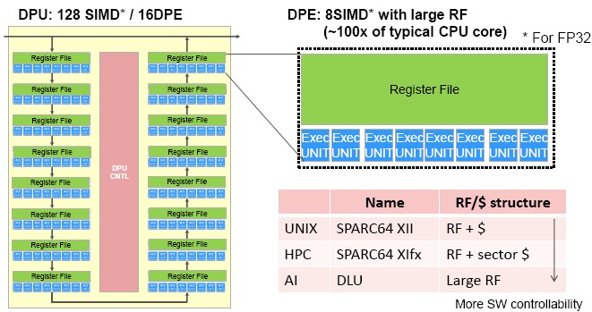
The initial DPU will have sixteen DPEs and a large register file instead of the cache hierarchy we see in CPUs and GPUs. Interestingly, that register file will be fully controllable through software, which will allow for the performance of the DLU to be extracted more fully than statically configured caches on CPUs, according to Maruyama. Each of the DPEs on the DLU has that large register file and eight SIMD execution units, for a total of 128 SIMD units per DPU.
The DLU will have a new data format called deep learning integer, according to Maruyama, which will support FP32 and FP16 modes as well as INT16 and INT8 modes; the 8-bit modes double pump the 16-bit integer units, and the 16-bit floating point modes double pump the 32-bit floating point units.
What is not yet clear is how many DPUs Fujitsu can cram on the die and how much HBM2 memory it can interconnect with the package on an interposer, so we do not know how powerful the DLU will be. The initial DLU will require a host processor, like a Xeon, but the second generation DLU will include its own embedded host processor, almost certainly an ARM core or cores, given the Post-K architectural choice of ARM. Looking out further, Maruyama hints that other specialized processors for neuromorphic or combinatorial optimization processing could be added to a later DLU.
While Fujitsu makes a credible case that deep learning and HPC processing require very different architectures to run efficiently, it is significant that both the Post-K and DLU units will speak Tofu, and in the event that the HPC and AI workloads converge – as we have discussed many times, with machine learning models and projected datasets filling in for parts of simulations to speed up the whole simulation – Fujitsu will still be able to sell a single box that can do both. And that, ironically, is a kind of convergence.

Arm And Japan Get Their Day In The HPC Sun
There is a constant push and pull between budget and architecture in supercomputing, and the passing of time has not made anyone’s arms tired as yet on both sides of the bargaining table. And the thing that is refreshing about all of this is that mixed in with all of …
Japan Buys Supercomputer Just To Predict Torrential Downpours
You know that climate change is a problem when a supercomputer to do short-term prediction of the formation of linear rainbands and the torrential downpours that they cause is 3.4X as powerful as the machines that do the day-to-day weather forecasting in a country. But this is precisely the situation …
Fugaku Remakes Exascale Computing In Its Own Image
When originally conceived, Japan’s Post-K supercomputer was supposed to be the country’s first exascale system. Developed by Fujitsu and the RIKEN Center for Computational Science, the system, now known as Fugaku, is designed to be two orders of magnitude faster than its predecessor, the 11.3-petaflops (peak) K computer. But a …
The SPARC64 XIfx actually doesn’t use an interposer. The HMC is mounted separately on the board from the CPU itself and both the CPU and HMC are covered by a Fujikura made copper coldplate.
This separate approach to processing HPC simulations and AI workloads gets around the inefficiencies that heterogeneous systems typically have, avoiding the idle time that CPUs in heterogeneous systems with LOCs and TOCs typically have.
It also lets one machine, or one section of a cluster of Post-K and DLUs, do the HPC simulation, then do the data reduction AI stuff on the other half. With all of it using Tofu that should scale incredibly well considering how well Tofu machines do in Graph500 and HPCG.
You lost me at Sparc (and I’m someone who actually once wrote dgemm in Sparc assembly). Tofu is not a great name marketing-wise. Otherwise, nice article.