It is convenient, perhaps, that large scale computing evolved just about the time the easiest and biggest strikes for oil and natural gas were over. Since the 1950s, energy companies have always been early adopters of advanced computing, networking, and storage technologies because accurate seismic processing to reveal the structures of the depths of the Earth’s crust is the only practical way to find oil and natural gas and manage their reservoirs of those hydrocarbons.
As The Next Platform pointed out earlier this week from the Rice Oil & Gas Workshop in Houston, the oil and gas majors were among the enthusiastic early users of Tesla GPU accelerator cards from Nvidia to boost the performance of their reservoir modeling applications, particularly those based on reverse time migration (RTM) algorithms that require lots of bandwidth. Before these GPU accelerators came along, the energy companies experimented with FPGA and DSP coprocessors, too, and we think there is good reason to believe that FPGAs might come around again, especially now that Intel has acquired Altera and the OpenPower collective is working on integrating GPU and FPGA accelerators tightly with IBM’s Power processors.
But at the moment, the hybrid CPU-GPU machines seem to be the preferred means of accelerating RTM applications compared to running the RTM code on plain vanilla X86 nodes that are clustered. The oil and gas majors are pretty secretive about the processors and coprocessors they deploy for their seismic analysis and reservoir modeling applications, but we understand that they tend to go with a combination of midrange Xeon processors (which offer the best bang for the buck) and fairly hefty GPU accelerators (which do the same) to build their hybrid cluster nodes. But this is not the only approach available. Both Intel and AMD sell hybrid workstation-class processors that put CPUs and GPUs on the same die or package and, practically speaking, put a hybrid server node into a single socket. While neither the CPU nor GPU are particularly powerful, they are fairly energy efficient devices and they are also higher volume and lower cost parts, too, which can mean that the cost per flops per watt of a cluster built using these hybrid chips in fairly wimpy server nodes can be better than for machines using beefier nodes.
Issam Said, who did his PhD thesis at the Sorbonne on hybrid chips running RTM applications and who is now a researcher at Laboratoire d’Informatique de Paris working with French oil giant Total, presented a paper at the Rice workshop comparing and contrasting clusters running Xeon E5 processors, hybrid Xeon-Tesla compute, and AMD’s “Kaveri” A-Series APU hybrid chips. Some of the iron that Said used in his comparisons was a little long in the tooth, but that is not the point. What is interesting is how the results of his benchmark tests show that you cannot simply dismiss the APU approach out of hand, and it also points to a possible future where AMD, with significantly beefier APUs based on its “Zen” Opteron cores and an integrated GPU plus high bandwidth memory, might be able to take on hybrid clusters that put discrete CPUs and GPUs into systems and perhaps blunt an attack from Intel with hybrid chips that put Xeon cores and FPGA accelerators on a single die. Intel could even get more aggressive with “Broadwell” and “Skylake” Xeon E3 processors that have their own integrated GPUs on the die, but has thus far seemed unenthusiastic about such acceleration and seems more inclined to push its “Knights Landing” Xeon Phi processor to customer that need lots of cores as well as fast networking and very large memory bandwidth – which describes RTM applications pretty well, as it turns out.
Suffice it to say, the oil and gas giants have plenty of options coming down the pike, and they are looking at them all, as Total explained in its keynote at the Rice workshop, despite an oil glut that has slashed the price of a barrel of oil to levels that are painful for the energy industry.
Wimpy APUs Versus Brawny CPUs And GPUs
For a long time, RTM applications ran on CPU clusters with lots of nodes, but in recent years, these applications have been accelerated and, according to Said, GPUs have come to dominate among those oil and gas companies (or service providers who handle some of their work) that have chosen to accelerate their RTM code. Said elaborated the reasons why GPUs have come to dominate among the accelerated RTM code, with high compute capacity – on the order of 5 teraflops per device – and high internal memory bandwidth – up to 300 GB/sec – being the two most important ones. However, there are issues when it comes to GPUs and RTM code. With the GPUs hooked into the CPUs by the PCI-Express bus in the server and with a sustained bandwidth of around 12 GB/sec, the PCI bus is a bottleneck. Moreover, a CPU-GPU pair consumes on the order of 400 watts. Said says that there are software approaches that can help mitigate some of these issues, such as temporal blocking and overlapping CPU-to-GPU transfers that can lower the PCI bus overhead and out-of-core algorithms that can deal with the limited memory in the GPU accelerators, for the purposes of the research performed at LIP6 on behalf of Total, Said wanted to throw hardware at the problem and see if an APU approach could fix some of these issues without resorting to software changes.
The advantages of the APU hybrid chips are that the GPUs can address the entire main memory of the processing complex and do not have to move data over a PCI-Express bus from main memory to GPU memory and back again. The APUs top out at about 95 watts, which compares favorably to CPUs typically used in HPC clusters, which peak at 115 watts, and GPUs that peak at 300 watts. There are drawbacks, however. The “Southern Islands” GPU embedded in the “Kaveri” A-Series A10 APU from AMD has about 730 gigaflops, which bests the performance of the eight-core “Sandy Bridge” Xeon E5-2670 v1 chip, which can handle about 332 gigaflops running at its base speed of 2.6 GHz. The Tesla K40 accelerator delivers 4.29 teraflops. (These are peak theoretical single precision floating point math ratings, and a lot of the workloads at oil and gas companies rely on single precision, rather than the more expensive double precision, math.) The Kaveri APU also has only about 25 GB/sec of memory bandwidth across the “Onion” bus that links the CPU cores to the GPU, which is more than an order of magnitude less than the 300 GB/sec between the parallel GPU and its GDDR5 frame buffer memory.
In past comparisons, Said has examined the use of OpenACC and OpenCL to compare various parallel computing approaches, but for the comparisons presented at the Rice workshop, the processor-only setups use Fortran90 code and Message Passing Interface (MPI) to allow code to share data across the cluster. The API uses the same stack, but uses OpenCL to distribute work and data to the GPUs. The GPU implementation, interestingly enough, uses the same code but does explicit copies between the CPU and GPU. The specific RTM model is called the 3D SEG/EAGE Salt velocity model, and as the name suggests, it does imaging underneath the salt domes below the Earth’s surface where oil is commonly found. In the tests, the CPU-only node had two of the Xeon E5-2670 processors. The Xeon-Tesla hybrid had a single Xeon E5-2680 processor (which has eight cores running at 2.7 GHz) married to a single K40 accelerator. And the APU node had just one Kaveri chip each.
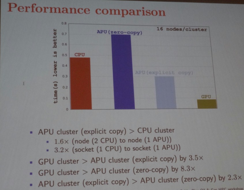
With sixteen nodes in each scenario, here is the time it took for the RTM model to run:
For the APUs, Said tested two scenarios. One where the hardware did the moving of data and another where the software told the hardware explicitly to move data between the two elements of the APU. As you can see below, that explicit copying helped improve the performance of the APU significantly. But, as you can also see, the CPU-only and CPU-GPU hybrid setups significantly beat the APU in terms of performance.
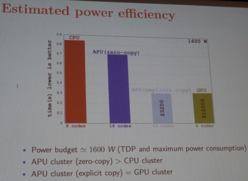
However, the story is not over. Said wondered what would happen if the node was restricted to a 1,600 watt power envelope per node – the level at which a 16-node APU cluster runs. That would be eight nodes of the CPU-only setup and four nodes of the CPU-GPU hybrid. And here is what that looks like:
With the explicit copy implemented on the APUs, the performance of the APU and the CPU-GPU hybrid are essentially the same when they have the same thermal constraints, but the APU setup costs $3,200 and the CPU-GPU hybrid costs $12,000. Both offer significantly better performance per watt than the Sandy Bridge Xeon nodes tested, but Intel has launched two generations of chips since then and is readying a third sometime soon with the impending “Broadwell” launch. Nvidia is also readying its own “Pascal” Tesla accelerators, and AMD has its “Carrizo” APUs in the field and will have a large-scale APU aimed at HPC workloads coming to market perhaps in late 2017 or early 2018 that will presumably make both Kaveri and Carrizo look like toys. This data is not intended to be used to make buying decisions, but rather to inform HPC shops in the oil and gas industry – and indeed, other industries – that they have to do the math and look at all possible ways to get flops and memory bandwidth for their code. This will be particularly true this year and next, when so much new hardware is going to be coming into the field.


It’s the Future workstation Zen/Polaris/other APUs on an interposer that will define AMD’s next professional computing platform that will see the Zen Cores wired to the Polaris/other GPU accelerator via the interposer that will have much better total effective bandwidth with the Zen Cores and Polaris accelerator having a much wider (HBM wide style) connection via thousands of interposer traces between CPU/cores and GPU! If AMD can currently wire its GPUs to HBM memory with trace counts of 4096 total traces(1024 per HBM stack) just imagine an APU on an Interposer with the Zen Cores wired directly to the Polaris GPU with an even wider than 4096 bit wide direct connection via the interposer. And AMD doing this with a separately fabbed Zen Die with 32 zen cores possibly sharing a memory controller/ultra wide coherency fabric with the Polaris GPU accelerator, and a very large Polaris GPU at that with thousands of GPU cores.
So it’s quite possible for the Zen cores to maybe transfer whole CPU cache lines with the GPU via a large enough direct amount of parallel traces to and from the Zen cores to the Polaris GPU accelerator via the interposer’s ability to host hundreds of thousands of traces, something that can not be done economically via a PCB if it can be done at all via the PCB. So a new APU on an interposer makes its appearance with Zen cores able to transfer whole blocks of data/other information between Zen cores and Polaris GPU ACE units in addition to the HBM stack’s own dedicated traces all happily hosted atop the interposer’s silicon and as many traces as one can get using the current silicon processes. And suddenly the potential of having thousands of parallel communication traces being able to be clocked at a much lower and power saving clock rate and still able to achieve better effective bandwidth than PCIe or GDDR5 at its 7 times the power hungry clock rate compared to what AMD does with HBM and whatever fabric AMD uses for its HPC/Workstation, and exascale, APUs on an interposer.
AMD even has that patent application to place some FPGA compute directly onto the HBM stack/s, between the HBM’s control logic die below and the HBM memory die stacks above for some in HBM memory distributed compute. And that “ “Kaveri” A-Series A10 APU from AMD has about 730 gigaflops” has already been supplanted by “Carrizo” APUs. And “Carrizo” which by the end of this year going to be supplanted by “Zen” and AMD’s HPC/Workstation and purposed Exascale class APUs on an interposer based systems that will be coming online over the next few years. So hopefully there will be, or be shortly, some workstation/HPC Zen/Polaris APUs on an interposer engineering samples making their way to researchers around the world to evaluate AMD’s newest products using its newest x86 micro-architecture with its newest GCN GPU micro-architecture. AMD’s APU’s on an interposer will be a bit more powerful than those single die APU based systems that are currently available for mostly the consumer market.
That “Onion” (1) bus already has a replacement with AMD announcing a new coherent interconnect for its HPC/workstation and exascale offerings, and just how future AMD APUs on an interposer will make use of HBM, in addition to secondary RAM(DIMM Based/other) is still not fully known. I’d expect that things for AMD might evolve towards most of the compute being relegated to the CPU/GPU/FPGA/Other processor based dies being hosted/wired up via the interposer along with HBM primary memory/RAM with the interposer becoming the new main-board of sorts and some form of interconnect fabric running between the interposer complexes with the PCB mainly hosting that and the power traces, optical traces(in the long term), and probably starting out with even some regular DIMM traces for secondary memory to RAM(DIMMs) based systems at first until future HBM versions allow for multi-TB+ of HBM. The first generation of APUs on an interposer will probably be slotted into mainboards the traditional way, and gradually evolve towards some form of optical only interconnect between the interposer modules with the PCB only hosting the power traces/power conditioning circuits to power the interposer modules with the remaining compute/memory fully hosted on the interposer module.
Note: the Polaris naming has supplanted the Greenland naming.
1.
http://www.eweek.com/servers/amd-developing-32-core-zen-apu-for-supercomputers.html
The use of APUs is interesting, but it looks like the GPU is being used inefficiently in the current CPU-GPU systems. That seems to be because their data set is too large to be stored on the GPU’s memory. But not mentioned in this article is that KNL Xeon Phi will have full speed access to main memory, and, if the oil and gas companies are willing to use Power 8+ CPUs instead of Xeons, Nvidia’s Pascal architecture will have NVLink and unified memory available also allowing it full speed access to main memory. The memory bandwidths will then be 2-3 times faster than the 25 GB/s listed for the “Onion” bus, and AMD could at best match it with future improvements since these architectures (KNL and NVLink) can access the main memory at full speed. The GPU still will be used inefficiently but more efficiently than current GPU implementations (without software optimizations). Bandwidth will increase 4-5x and single precision peak performance of Pascal will increase about 3x over the K40 implementation. If AMD doesn’t come out with better APUs until 2018 they will have to compete with Knights Hill and Volta.
Mr Pritchard, I’m puzzled by your statement. The APU with explicit copy beat the CPU only run every time, didn’t it? Your text suggests it didn’t. Did I misread the chart?