
The new Intel “Knights Landing” processor’s topology includes what it calls near memory, an up to 16 GB block of on-package memory accessible faster and with higher bandwidth than traditional main memory. Near memory is distinct from the up to 384 GB of main memory supported on the Knights Landing chip. This new memory architecture presents some interesting options for applications running on high performance systems.
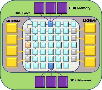
The processor and memory topology of Knights Landing can be seen in the following figure. The MCDRAM is near memory and DDR4 is the far memory in the system.
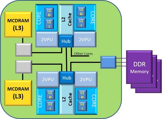
But what is this near memory really, and how/when would an application want to use it? Intel does not yet provide a lot of information, but here is a block diagram to show what the Knights Landing architecture looks like:
And here is what we do and do not seem to know:
- The near memory (also known as on-package memory) was jointly developed by Intel and Micron Technology. This High Bandwidth Memory (HBM) will be up to 16 GB in size at launch. This is on-package, not on-chip.
- The near memory link’s bandwidth will be about 4.5X to 5X higher than that of DDR4 memory. This appears to be total bandwidth, as shown in the above figure, with all channels – both MCDRAM and DDR memory – populated. As reported previous in The Next Platform: “The HBM on the package has around 400 GB/sec of aggregate bandwidth across eight segments of 2 GB of memory using a proprietary link. The two DDR memory controllers on the chip have around 90 GB/sec of bandwidth and max out at 384 GB of capacity. So it is 4.5X the bandwidth for HBM than DDR4.”
- Given a cache miss on a core, and assuming low memory-bus utilization, the latency of that cache miss sourced from MCDRAM is still unknown. The MCDRAM’s access latency, though, is assumed to be considerably faster than that of a similar DDR memory access. The relative difference would, though, need to be some function of the bandwidth and on the same order of magnitude as any benchmark heavily exercising relative memory accesses.
- Each core has 32 KB each of L1 data and instruction cache. Pairs of cores share a 1 MB L2 cache kept coherent across all cores. (We’ll be discussing cache concepts shortly.)
- The MCDRAM can be used in one of three different modes (with mode set at system restart):
- Cache mode: The MCDRAM units together acts as a shared (up to 16 GB) L3 cache, a cache common to all of the chip’s cores. We will be assuming that this L3 cache acts as a cast-out cache. Any data, including both changed and unmodified, that is cast out of a core-pair’s L2 cache is first written by the hardware into the L3 cache. More on this later. It seems to follow, though, that each MCDRAM controller – shown as grey in the figure above – has an L3 cache directory for identifying which real memory data blocks reside in each MCDRAM.
- Flat Model mode: The MCDRAM acts as memory in its own right. The DDR memory and the MCDRAM are addressed with separate real addresses. Both the Flat Model MCDRAM and DDR memory are accessible from the processors. Unlike the L3-mode MCDRAM, wherein the hardware decides what resides in the MCDRAM, the applications and the operating system decides – via virtual and real addressing – what resides in each type of memory.
- Hybrid mode: Portions of the MCDRAM act as L3 cache. How this differentiation is decided is not clear at this writing.
- The setting of these modes is controlled strictly at system boot time; you need to decide what setting works best for your use.
- Whether the MCDRAM mode is set up for a cache or as memory, an L2 cache miss may find its data there; the latency of access from MCDRAM on such a cache miss is assumed to be the same, independent of mode.
Simply because MCDRAM can exist as an L3 cache, an MCDRAM access would need to be considerably faster than a similar access from the DDR memory. At this writing, Intel has only published the likely associated bus bandwidths; we do not know the latencies. So, for now, we guess. So let’s say the relative difference is a factor of 4X. (Again, this is only a guesstimate, intended only to provide you with a mental model.)
So, given the above, under what circumstances do we decide to use each of these modes? It happens that knowing this stuff is not enough, but it is a start.
The MCDRAM and its massive bandwidth links exist for reasons of performance. Given that cores incur an L2 cache miss, we assume your application’s performance would be better served by cache fill from the MCDRAM, no matter what the mode. Better served, yes, but let’s keep in mind that good performance does not require that all accesses come from the MCDRAM any more than it requires that all accesses succeed in hitting on the L2 cache. It’s a probability thing, the cases of which we will get into shortly; the higher the probability of an access from a faster location, the better the performance of the application.
- As an L3 cache, you control very indirectly how much of your data resides in the cache. You want to minimally access the DDR memory and maximize a core’s accesses from its own L1 and L2 caches.
- As Flat Model memory, you choose what data objects are going to reside there such that your application perceives a high probability of MCDRAM accesses versus DDR memory. Even so, here too, you want to maximize the L1 and L2 hit rate.
That sort of thing is what we will be covering in what follows.
Some Quick Cache Theory
So that we are all on the same page, let’s go over why it is that cache of any type improves performance.
Caches are intended to be much more rapidly accessed than DDR memory. Each type of cache is segmented into regions called cache lines, each with the purpose of holding some contiguous data block – say, 64 bytes on a 64-byte boundary – representing the contents of an equal-size DDR memory block. Knights Landing, and many other modern processor designs come with different types of caches, each with a different speed and size. In Knights Landing there are
- L1 data and instruction caches, 32 KB each in size, one each per core,
- L2 data cache, 1 MB in size, common to pairs of cores (and the one to eight threads executing there),
- Optionally, an MCDRAM-based L3, up to 16 GB in size, common to all of the cores on the chip. As shown earlier, this total cache is physically made up of eight regions, each with a controller and link.
The L1 cache accesses are typically completed in one or two processor cycles; think fractions of nanoseconds for L1 accesses with DDR accesses taking hundreds of nanoseconds. L2 access latencies are slightly slower than L1; think a small handful of cycles (for example, less than ten). L3 accesses, being still further away from the cores (and indeed off chip), take still longer. Again, an access from DDR memory takes multiple times longer than MCDRAM accesses.
It does not matter how few bytes of a block (i.e., cache line) your application actually accesses, if the data is not in that cache, the cache controller requests a complete block’s worth of data from a slower level of storage.
We understand that the on-core L1 cache line size is 64 bytes. The 32 KB L1 caches are segmented into these 64-byte blocks, typically as a two-dimensional array of such blocks; one dimension exists for aging, keeping the more frequently accessed blocks in the cache longer. (But we don’t yet know that for Knights Landing.) As you would want, typically most data and instruction stream accesses succeed in coming out of this L1 cache. Most accesses, yes, but when the needed data is not in the L1 cache, your application starts to experience time delays, the worst being when it needs to wait for data to be brought out of the DDR memory.
In the event that the L1 cache is accessed and the needed data or instructions are not there, a 64-byte cache fill request is sent to the core-pair’s L2 cache. If the L2 happens to have that memory block, the L2 responds back to the core relatively quickly with the needed 64-byte data block, filling a L1 cache line with its contents. Think of instruction processing as being paused for only a few processor cycles to accomplish this.
Let’s pause for a moment to observe that the L2 cache line size might also be 64 bytes in size, but it might be 128 bytes or even 256 bytes in size. Even so, whatever the L2 cache line size, with a L1 cache fill request, given the needed data is in that core-pair’s L2, the L2 cache responds with the needed 64 bytes.
Similarly, if such an L2 cache access finds that the needed data block is not in that L2 either, the L2’s controller similarly makes an access request – this time of size equal to the L2 cache line size – from still slower memory. For example, referring to the figure above, this access request may have its data block served from another core’s L2, from the MCDRAM – whether in L3 cache mode or Flat model mode – or from DDR memory.
Even if your program accessed a single byte of a requested block, the cache fill access is a complete block’s worth in size. No matter that your program might be randomly accessing independent bytes all over memory (and so you might be thinking that the L1 cache can hold 32K of such bytes), the number of independent blocks in each cache is actually no more than the size of the cache divided by the cache line size. For example,
# of L1 Data cache lines = 32 KB / 64 bytes = 512 L1 cache lines
So, at any moment in time, the L1 data cache can only hold 512 different blocks of memory. As a new block is filled into the cache, another block must be removed.
As data gets changed, the changed data continues to reside in the cache (typically L2) for a while; it is typical that the change is not immediately returned to the DRAM. As more data blocks are pulled into the cache, even aged changed blocks must be removed from that cache. Such changed block’s entire contents – no matter that, perhaps, only one byte had been changed – must then be written out of that cache. What happens next with that changed block depends on whether the MCDRAM is in L3 cache mode or Flat model mode. (As a bit of a warning, what follows is going to feel a bit esoteric, but what we are trying to first show is the physical differences between using this MCDRAM as a cache versus as real memory. From there we get a better feel for the performance trade-offs.)
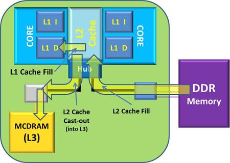
L3 Cache Mode: I have said that when new data blocks are pulled into the L2 cache, the previous contents of the selected cache line is either written out (if the cache line is changed) or perhaps simply lost (if unchanged). It is typical, though, that the L3 cache acts to hold any data blocks cast out of the L2 cache(s). Changed or not, data blocks cast out of the L2 are stored into the L3 cache, where the data block gets to live in a cache – albeit a slower cache – for a while longer.
So, in the event a core-pair’s subsequent L2 cache miss, the resulting cache fill request might find it’s needed data still in the relatively faster L3 cache – here, the MCDRAM – rather than having to request the data from slower DDR memory. And there can be a lot of data blocks in there. Given the L3 cache line size is 128 bytes, the number of these cache lines is
# of L3 cache lines = 16 GB / 128 byte lines = 134217728 blocks = 128 mega-lines
Notice that these L3 cache lines have been fed with the cast out contents of any and all of the L2 caches on this processor chip.
The total L3 may be a wonderfully large data state, but it came at a cost. Being a cast-out cache, every single data block cast out of any L2 cache is written into the L3 cache, that is if the block is not already in the L3 cache. Given a rapid L2 cache fill rate, the internal busses as well as the links to the L3 caches are experiencing a similarly significant traffic. Overuse of any resource typically means delayed access of any subsequent uses of that resource.
Referring to the first figure of this story, notice that there are also up to eight MCDRAM controllers, each one associated with one unit of MCDRAM. These MCDRAM controllers will decide which cast out blocks go into what MCDRAM unit. These controllers also know, upon an L2 cache miss, whether their portion of the L3 cache has the requested data block. With any luck, both the data blocks cast out and being filled are spread out evenly over each of the eight MCDRAM. It would seem that there is such a look up on these directories for each block cast out of the L2 caches.
The theory behind such a cast-out L3 is that any block previously held in any L2 cache will again be soon needed by a core. The extent to which this is true is what makes the L3 useful (or not). For examples, suppose:
- After a program changes a data block in the L2, that changed block is cast out from there into an L3. That block is not soon re-accessed, so it ages there. Because other blocks are subsequently flowing into the L3, that changed block is aged out of the L3 to make space. So the changed block must be read out of the L3 and written back into its home location in the DDR memory. The cast-out into the L3 was not useful and required extra processing to return the changes to DDR memory.
- As a slight variation on the previous, suppose the data block in the L2 had been unchanged and then cast-out into the L3. Lack of re-access means that it is similarly subsequently aged out of the L3; the unchanged block is thrown away. In either case, the hardware is spending bus resource to process a data block through the L3 that is not being used (before being lost).
- As a counter-example to the previous cases, suppose that a changed block was cast out to the L3 and shortly thereafter another core wants access to that same data block. The L2 cache fill is done from the L3, re-accessing this changed data block. This might be done repeatedly over an extended period of time, avoiding any (re)access of the data block in the DDR memory. Here the cast-out process was useful, and further avoided the latency of a DDR memory access.
Before going on, recall that this L3 cache contains copies – or modified versions – of up to 16 GB of blocks of DDR memory. If the relatively frequently used working set largely fits in this space, the DDR memory may be very infrequently accessed which is a very good thing.
It is worth observing that the L3 cache backs up the L2 cache. For those periods where the current contents of the L2 cache is being completely successful in feeding the processor, the L3 cache provides no service. It’s because the L2 cache is often not big enough that more data blocks are needed and so more are cast out into the L3. The rate of fill – and so cast-outs – varies based on the current working set from very low to very high and everything in between. (As we’ll see later, you can influence this.)
Flat Model Mode: The MCDRAM here is not an L3 cache, it is memory in its own right, with its own portion of real address space. It’s just faster memory than DDR memory. L2 caches still cast out changed data blocks, though, the target of those changed data blocks might be either the MCDRAM or the DDR memory. Whatever location acted originally as the source of the L2 cache fill, that same location acts as the target for the cast-out block.
What is not happening is that the hardware does not automatically guide changed blocks from the MCDRAM memory into the DDR memory; your program might, cast unchanged data blocks into the MCDRAM, cast changed L2 cache blocks originally sourced from DDR memory into the MCDRAM.
Similarly, as with DDR memory, the MCDRAM memory acts as the source of data blocks for cache fills targeting a core-pair’s L2 cache. The key here is that any such cache fills from MCDRAM memory are completed faster than from the DDR memory; such MCDRAM-sourced fills are assumed to be done just as fast as from MCDRAM-based L3.
Because the application is taking responsibility for what resides in the MCDRAM, the hardware need not. As a result, hardware resources used to otherwise maintain the L3 cache remain free for cases where they are needed. Further, such pre=knowledge on the part of the application can result in a higher success rate on accessing from the faster MCDRAM.
As a conclusion concerning cache theory, it’s worth noting that cache improves performance because of both storage locality and temporal locality. For storage locality, the cache designs assume that if your program is going to access even a byte, then your program is likely to need to access some number of the bytes immediately around it. Again, on an L1 cache miss, even though your program accessed – say – an integer, the hardware is going to fill an L1 cache line with 64 bytes which includes your integer. The cache design is successful when your program accesses data around it. Where this is not true, the benefit of the cache is lessened. For temporal locality, cache design assumes that your program will continue to (re)access one or more data items in a cache line frequently enough to keep that block in the cache. When the program is perceived as not accessing that block, the block disappears from the cache. “Frequently enough,” though, is dependent upon how quickly new cache lines are being pulled into the cache; the faster that data blocks are pulled into the cache, the shorter the time that another data block remains in the cache for subsequent reaccess.
The Trade-Offs
How do we decide using the L3 cache approach versus Flat Model memory? 16 GB seems like a wonderfully huge cache, and it is! The question on the table, though, is “Can pre-knowledge of our application’s data use – and, perhaps, even reorganization of that data – allow our application to run still faster if we instead use Flat Model mode?”
With the Flat Model, we, rather than the hardware, manage that which will reside in the MCDRAM near memory. With hardware doing the managing (as a cache), the hardware saves everything there that no longer fits in the L2 caches whether or not it will be reused; essentially everything that gets accessed would ultimately flow through this L3. With the application managing the MCDRAM, you decide, mostly based on your perception of frequency of access there. It is frequency of access from the MCDRAM that is important; recall that for some applications the L2 cache(s) can (and preferably will) hold the data blocks for a while.
Flat Model mode memory is memory, just like any other addressable memory. With MCDRAM, perhaps in ways similar to NUMA-based topology systems, we have multiple speeds of memory. It can also be virtual memory, managed as pages; some interface into the OS decides that some virtually-addressed pages will be mapped onto MCDRAM memory rather than DDR memory. Indeed, you may recall from this Intel Knights Landing presentation that Intel is proposing a heap manager interface, which allows your programs to allocate from MCDRAM memory; this hbw_malloc returns the virtual address of an allocated region in MCDRAM.
Although, at 16 GB, the MCDRAM memory is certainly large, it is nonetheless a fraction of the potential 384 GB of the DDR far memory memory. The trick is getting that which is most frequently accessed – and incapable of staying in the L2(s), to reside in this Flat Model mode MCDRAM memory. You don’t need everything being accessed to reside there. Performance is all about frequency of access; that which is infrequently access can be accessed from slower memory and only minimally impact performance.
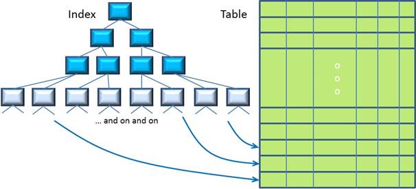
For example, and we’ll be getting into this shortly, consider a straightforward search of a massive database table fronted by a large index. The DBMS tends to only touch the portion of the table proper which contains the row(s) actually being accessed as the result. Think of this as a single touch and so low frequency. On the other hand, the query – or even many queries – will be repeatedly touching portions of the index. It is the index that should reside in the MCDRAM, not necessarily the table.
Efficient Use Of Memory And Cache
Given we are using the MCDRAM in Flat Model mode, we nonetheless want to maximize the amount of relatively frequently accessed data that resides there. But, even if we weren’t, we also want to efficiently use the 1 MB L2 caches, keeping more frequently accessed data blocks there and minimizing the number of cache fills into it (which, we know, knocks other blocks out of the L2).
The key to this is data organization; how would the data objects and program instructions get mapped into pages or cache lines?
As a straightforward example, consider a linked list as in the following:
For most programmers this diagram is just how we think about it (and no further).
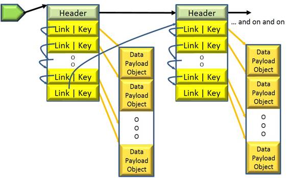
Each item in the list is an object, taking up some amount of storage. But where? All that is usually known for sure is that the storage is somewhere in a software abstraction called the heap. The generic heap manager doing this storage allocation has no idea that each was going to be part of a linked list; it will just allocate the needed storage as efficiently as possible from its point of view. The result is that, as your program scans through the list, each node is likely being found in a different block of memory, perhaps even in a different page of memory. Each is going to effectively consume a cache line when it is accessed, meaning a cache fill for each, and then be knocked out of the cache as other objects are pulled in. For a moderately long list, by the time the processor gets to the end of the list, the first part of it – and everything else that had been in the L1 before – is no longer in the L1 cache. It is also worth observing that the Link-Key object may be just a few bytes in size, a small fraction of the 64-byte L1 cache line size. Other stuff may be in the remaining bytes, but what, and is it useful now?
The following figure is functionally the same linked list. Here, instead of allowing some generic heap manager allocate memory, the nodes of the list are organized as part of array-like storage. It’s not that this needs to be perceived as an array – each node can be pointing to another as before – it just that the virtual and physical storage backing these nodes are contiguous blocks of memory, nodes contiguous within data blocks. Here the same information is packed tighter in both the Fixed-Model MCDRAM and in the L1/L2 caches. Tighter packing means fewer cache fills – even if from this faster MCDRAM – and so still faster operations on this list, more space for other data in the caches, and more space for other data in the MCDRAM.
(Note: Think of these linked arrays abstractly as one large and growable array. The “Link” values are then just indexes into that abstract array.)
I will not take you through the details here, but mentally picture the same game with the nodes of a database index or any tree structure. The basic unit of virtual / physical storage to use is some multiple of the cache line size. Many such nodes are considerably smaller in size. Can the same information be repackaged and have an associated storage manager which is more friendly to cache and MCDRAM?
Conclusion
I can imagine whole books being written on such optimizations, and you certainly don’t want to read much more of it here. Notice, though, where we have been in this article. We started with a physical construct, DDR memory and the faster MCDRAM as seen in the Knights Landing design. We realized that hardly any programmers work directly with such physical constructs. Instead, the MCDRAM is virtual memory mapped onto this faster physical memory or it is just an L3 cache, which most programmers hardly realize – or for that matter, hardly need to realize – exists. We then moved up the stack to concepts that programmers do appreciate and noted that you do have some control over the appropriate use of this new hardware feature, allowing your applications to really scream when needed.
After degrees in physics and electrical engineering, a number of pre-PowerPC processor development projects, a short stint in Japan on IBM’s first Japanese personal computer, a tour through the OS/400 and IBM i operating system, compiler, and cluster development, and a rather long stay in Power Systems performance that allowed him to play with architecture and performance at a lot of levels – all told about 35 years and a lot of development processes with IBM – Mark Funk entered academia to teach computer science. He is currently professor of computer science at Winona State University.
Reprinted with permission of Mark Funk. Original story posted here.




If MCDRAM latencies were significantly lower than DDR latencies, Intel would be advertising that, just as they are advertising the large increase in bandwidth relative to DDR. Significantly lower latencies would benefit any number of applications and it would serve no purpose for Intel to hide that fact.
Except to possibly save something for announcement day in the second half….
First, there’s no indication from memory vendors that latencies are going to decrease a lot. This would be a huge marketing issue for Intel to get out early so that they capture potential buyers whose workload is latency sensitive. If someone was about to procure a large system, they’d probably wait to get a product that would help them out significantly.
Jaia –
You’ll have noticed that the underlying tone of this article was one of conjecture. I’m, here, going to continue with that attitude.
All that we know for sure is what has been written so far. We know that the near memory is “on package”, that there are up to eight of them, and each has a point-to-point link back to the processor chip. As far as I can tell, Intel has not told us how that memory is packaged within those on-package – but off-chip – units.
So let’s again make an educated guess based on a real technology. Recall, first, that Knights Landing also offers this technology up as having a Cache mode which I called an L3 cache.
So let’s look at – for example – the L3 cache design of IBM’s POWER7. It is on chip, of a fair size, faster, and uses a technology that they call eDRAM. Wikipedia covers it here; http://en.wikipedia.org/wiki/EDRAM
Aside from IBM’s POWER7, that article describes a number of other products using eDRAM as well.
So, in conclusion, why couldn’t Knight Landing’s Near Memory use something similar? It would be more expensive than DRAM, but they are not populating their entire memory complex with this type of memory. And, again, recall that they offer a Cache mode, this large shared cache just happens to be off chip, reserving the otherwise used chip real estate
for more processors. Strikes me as a nice design and architecture trade-off.
And thanks for your interest.
Mark
I’m sure hardware guys like this a lot. But. A huge selling point of the Knights products has always been that you just recompile and BOOM! It works, and so do all your tools. Vector optimizations are needed, sure, but HPC guys have been doing that since the Cray-1 (possibly earlier). This appears to toss that selling point in the dumper, putting Knights into the realm of GPUs – all the performance you want! Just rewrite all your code! Simple!