

We are hitting the limits of what can be crammed into DRAM in a number of application areas. As data volumes continue to mount, this limitation will be more keenly felt.
Accordingly, there has been a great deal of work recently to look to flash to create more efficient and capable system that can accelerate deeply data-intensive problems, but few things have gotten enough traction to filter their way into big news items. With that said, there are some potential breakthroughs on this front coming out of MIT where some rather impressive performance improvements have been snagged by taking a unique, scalable approach to tapping into the promise of flash.
Flash may hold the performance and efficiency key, but it lacks in other areas, including the fact that users have to carefully think about the number of overwrites they’re making and, for the large-scale data analytics crowd, there are some other sticky problems. According to MIT researcher, Arvind, flash might excel in random access capabilities over disk, “currently available off-the-shelf flash storage packaged as SSDs do not make effective use of flash storage because they incur a great amount of additional overhead during flash device management and network access.”
These limitations were the inspiration for a new architecture developed at MIT called BlueDBM, which Arvind tells The Next Platform will outperform existing flash-based approaches that don’t have the extensive features his team has architected by 10X for certain applications. At its simplest, BlueDBM is a flash based architecture with in-store processing potential and an engineered inter-controller network between storage devices. In short, they are moving an FPGA close to the storage—not a new concept by any means, but one where we can see a bit more of the under the covers work than in other cases.
The idea is not complex necessarily, but the execution is. More so than it might appear, as it turns out, particularly in terms of how BlueDBM is subverting the storage hierarchy through its unique approach to global addressing. And it does so in a manner that doesn’t require the developer to move things around; it goes well beyond a single node. The current system they have built, which uses Samsung SSDs and Xilinx FPGA boards is currently at 20 nodes, but that’s 20 TB and the “sky is the limit” scalability wise, according to one of the designers of the system, MIT’s Sang-Woo Jun.
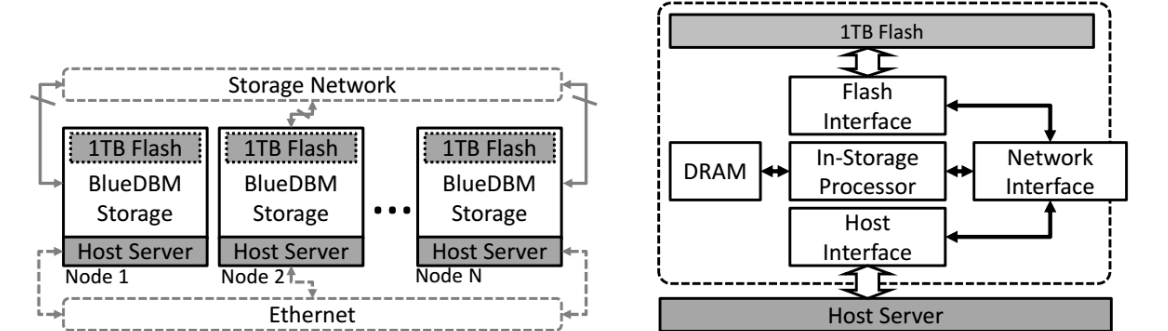
The current implementation is 20 nodes, but this is because of funding barriers versus a scalability wall. The system has proven itself on workloads up to 20 TB with uniformly low latency access into a network of storage devices to create a global address space. It can also make use of user-defined in-store processing engines (in this case it’s a Xilinx FPGA) and sports a design (manufactured through cooperation with Quanta Research as a donation) that can make application-specific optimizations in flash accesses.
“We are confident we can get to 100 nodes at least,” Jun says. “Our biggest scalability limit is that we are using an ad hoc mesh network work scheme in which all the nodes act as both switches and end nodes, but it doesn’t have to be this way if scale is the goal. It wouldn’t be difficult to use switches as in normal datacenters, but here that mesh is valuable because we didn’t want to spend time designing separate switch hardware.” The real limitation to scale is more likely to be reliability, however. There is not a lot that has been cooked in at this early stage to protect from failures. Still, at 20 nodes now, it is possible to solve problems that would take far higher node counts—that’s the real takeaway at this early point.
There have been other efforts with disk in particular and the placement of accelerators nearby, but the latencies were high and the accelerators did not boost performance enough for such efforts to catch on. Further, as Arvind tells us, there is an incredible amount of complexity baked into flash that the user is never aware of. It takes a 6-core ARM processor and 1 GB of DRAM just to manage flash storage and for a recent, large 32 TB installation he encountered, it took fourteen 4-core ARM processors and many GB of DRAM to keep it running. “Even though the whole package is tiny, it’s amazing how much it’s hiding. We are saying that an even simpler interface should be exposed that will be more efficient and let us use the underlying flash chips efficiently.”
This is key to their approach, which uses an in-store processing engine (FPGA-based) with a newly built abstraction layer. While such a layer doesn’t do much about hiding the inherent complexity of programming FPGAs (which Arvind recognizes is an issue), he says with such expertise, it is possible to make full, efficient use of flash and thereby drastically reduce the number of nodes required (and all the costs and failure potential that comes at scale).
Arvind and team have had conversations with all the major storage manufacturers. He cites Samsung (a major donor of parts for the project), Hynix, NetApp/EC, and others have shown interest because, “for them to understand end to end application performance is tough and this is valuable information.” They have also built a key value store on BlueDBM (similar to what Facebook uses for Memcached) and are also working on accelerator extensions to allow for work on very large sparse matrix problems. A far more detailed description from published MIT work can be found here.

Putting More Flex Into Flash Storage Arrays
In a cloud-based, highly distributed, and data-centric world, flexibility in what a piece of hardware and its systems software can do, where it can run, and how it can be configured is a critical differentiator for picky enterprises. For several years, Pure Storage has been talking about flexibility and choice …
The Pursuit Of Storage That Spans The Clouds
Every IT supplier has cloudy envy. And not just because utility-style pricing has become normalized by the big public clouds, but because they want to have a more regular, annuity-like revenue stream rather than always chasing the next deal. But don’t take that too far. Most large enterprises want to …
Hyperscalers Start Taking Pure Storage Flash For A Spin
Usually, innovation starts with the hyperscalers, HPC centers, and cloud builders of the world and spreads to the enterprise. But every once in a while, a technology establishes itself in large enterprises and the migrates upwards. This may be finally happening to Pure Storage, which was founded in 2009 and …
Be the first to comment