If there is any market on Earth that is sorely in need of intense some competition, it is the datacenter GPU market that is driving the AI revolution. Nvidia pretty much owns it.
But with every passing year, AMD’s Instinct GPU accelerators are getting more competitive, and with today’s launch of the Instinct MI325X and the MI355X, AMD can stand toe to toe with Nvidia’s “Hopper” H200 and “Blackwell” B100 at the GPU level.
But as AMD knows full well, people buy systems, complete with interconnects and systems software and AI frameworks as well as GPU accelerators, and here, Nvidia still has a decided advantage in many respects. But then again, if you can’t get Nvidia GPUs – as many companies cannot – then AMD GPUs will do a whole lot better than sitting on the sidelines of the GenAI boom. Moreover, AMD is catching up with CUDA with its ROCm stack and it has a plan with its UALink partners to come up with a coherent memory interconnect that can compete with Nvidia’s proprietary NVLink and NVSwitch fabric, allowing for rackscale and maybe even rowscale systems.
But today at the Advancing AI event in San Francisco, the unveiling of more details about the MI325X and MI355X and hints of the future MI400 are perhaps the most important things discussed. Everyone wants GPU accelerators with a wider range of mixed precision and more HBM memory capacity and bandwidth.
Let’s start with the MI325X, which has slightly different speeds and feeds from what was revealed to us at the Computex trade show in Taiwan back in June.
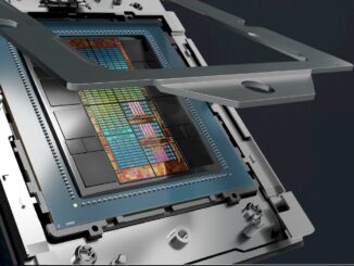
The speeds chart shown above says that the MI325X complex has 153 billion transistors, which is a tremendous number of transistors in a package. The floating point math performance of 1,307.4 teraflops at FP16 half-precision and 2,614.9 petaflops at FP8 quarter precision was exactly as advertised four months ago. However, the memory capacity on the MI325X is coming in a little light. Originally, AMD said to expect 288 GB across those eight stacks of HBM3E memory, but for some reason (probably having to do with the yield on twelve-high 3 GB of memory stacks) it only has 256 GB. The memory bandwidth is the same as was announced in June at 6 TB/sec across those eight HBM3E stacks.
The MI325X has the same performance as the existing “Antares” MI300X GPU, and in fact, the MI325 is the same compute complex, etched in the same 4 nanometer processes from Taiwan Semiconductor Manufacturing Co, with its power boosted from 750 watts to 1,000 watts to be able to drive more HBM memory capacity and higher bandwidth out of it.
The MI300X had 192 GB of slightly slower HBM3 memory, which had 5.3 TB/sec of aggregate bandwidth on the package. As far as we know, the 256 MB of Infinity Cache that sits between the GPU tiles and the HBM3 or HBM3E memory is the same.
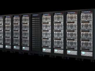
The MI325X plugs into the same sockets and into the same Open Compute universal baseboard server platforms as the MI300X did, so there is no need to create a new server design to accommodate these MI325Xs. You do have to have the thermal capacity to cool them, of course.
Here are the feeds and speeds of an eight-way GPU node using the MI325X:
Each MI300 series GPU has seven 128 GB/sec Infinity Fabric links, which allows them to be connected in an all-to-all, shared memory configuration inside of the node.
Lisa Su, AMD’s chief executive officer, said at the event that the MI325X would start shipping at the end of the current quarter and would be in the field in partner products in the first quarter of next year. This is more or less when Nvidia will be ramping up its Blackwell B100 GPUs, too.
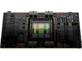
But for now, AMD is content to compare the MI325X against the fat-memoried Hopper H200 GPUs, which sport 141 GB of HBM3E memory with 4.8 TB/sec of bandwidth across its six stacks. Here, AMD has a 1.8X advantage in GPU memory capacity, which means it takes 1.8X fewer GPUs to load a particular model’s parameters, and a 1.25X advantage in bandwidth, which means it takes less time to feed those parameters to the GPUs. (It is interesting to contemplate the ratio of memory capacity to bandwidth on AI training performance, but we don’t have time for that right now. . . .)
Here are the benchmarks that Su showed off at the event, pitting the Mi325X against the H200:
On these three inference tests, it looks like performance is driven primarily by the bandwidth differences between the MI325X and the H200, with some wiggle here and there. The Mixtral benchmark shown at the left of the chart above is measuring inference throughput, where memory capacity might matter more, and the Mistral and Llama 3.1 tests are measuring inference latency, which seem to be driven by HBM bandwidth.
With eight GPU platforms, all of these benefits scale up proportionately:
And here are some performance specs for Llama 3.1 benchmarks with 70 billion and 405 billion parameters that bear this out:
We have been waiting to see some benchmarks for AI training, and AMD has finally given us two datapoints to work with, using the older Llama 2 models from Meta Platforms:
The interesting bit here for us is to see a 10 percent performance advantage for the MI325X over the H200 when a single device is used, but that advantage disappears when moving to an eight-way GPU node. Our guess is that Infinity Fabric is just not fast enough compared to the NVSwitch interconnects used in the Nvidia HGX machines, which help. But at performance parity, maybe NVSwitch and those big fat 900 GB/sec NVLink pipes in the H200 HGX complex don’t help as much as we thought. At least for Llama 2 inference.
Where is the Llama 3.1 training data, AMD? This is what matters right now.
With that, we shift gears to the Instinct MI350 series GPUs, which will be a family of products and the first of which, we learned today, will be the MI355X.
The MI350 series will implement the CDNA 4 architecture, which presumably was pulled in from the even more future MI400 series of datacenter GPUs expected in 2026. The MI350 series will be etched in a 3 nanometer process from TSMC, and will presumably have eight chiplets in a socket. (Ten would be too tall and skinny, unless you make the chiplets rectangles laid on their side.)
As was revealed back in June, the MI350 series will be the first GPUs from AMD to support FP4 and FP6 floating point data formats, and they will have the full complement of 288 GB of HBM3E memory using twelve-high stacks of 3 GB. It will have 8 TB/sec of bandwidth for that HBM3E memory, which presumably will be in eight stacks.
Whatever is going on with the CDNA 4 architecture, the MI355X socket is going to deliver 1.8X the performance of the MI325X, which is 2.3 petaflops at FP16 precision and 4.6 petaflops at FP8 precision, and 9.2 petaflops at FP6 or FP4 precision. (That is not including sparsity matrix support, which makes the throughput twice as high if you don’t have a dense matrix you are doing math upon.)
This begs the question of whether or not the MI355X will be under-memoried relative to the MI325X. If the MI325X was balanced in terms of a compute to memory ratio at 288 GB and 6 TB/sec, then we would expect for the MI355X to have 512 GB of HBM3E memory capacity and 14.4 TB/sec of bandwidth out of that memory. And I think we can all agree that this would be a fabulous device.
Anyway, here are the feeds and speeds of an eight-way MI355X system board:
And this shows how the eight-way system boards across the MI300X, MI325X, and MI355X span performance ranges and parameter sizes:
Remember when 500 billion parameters sounded like a lot? Now, tens of trillions seems to be no big deal.
It will be interesting to see what the CDNA-Next architecture used in the MI400 series looks like, and what kind of crazy packaging AMD uses to cram more stuff into a socket. And we also would love to see the capacity planning that AMD is doing to try to steal more business away from Big Green. Everything is gated by HBM availability.


” Moreover, AMD is catching up with CUDA with its ROCm stack ”
This looks like a talking point being parroted. Some proof would be nice.
That wasn’t the point of the story, but I will be taking a look into ROCm 6.2, which is a hell of a long way better than the first couple of releases.
NVIDIA supports CUDA across the whole product line from commodity graphics cards, enthusiast gaming all the way to advanced GPU accelerators. As a result the software ecosystem is huge–lots of developers creating and debugging stuff at multiple levels in different ways.
On the other hand ROCm does not officially support any graphics card except the old Radeon VII and a few workstation cards. Generally you need a supercomputer with an Instinct accelerator and three assistants to maintain the development tools in order to write code. In particular, ROCm does not officially run on the commodity hardware needed to support a robust developer community.
Yes, I know that ROCm sort of works on Polaris and better graphics cards. No official support means a whole class of software–game physics, media editing and local AI inference–can not depend on ROCm. Fewer developers means less polish and less quality.
I think NVIDIA also spends a lot more money on CUDA and its libraries than AMD does on ROCm, but that’s a different story.
From a growing share perspective and opportunity, does it matter that ROCm is only most useful for the biggest hyperscale customers and the smaller AI startups? Growing into that market gives time for AMD to expand from both ends to support more of its devices as well as unify the stack across CPU and FPGA. With the Silo acquisition and others, AMD may find ways to use HSA to drive even better performance than just through GPU, allowing them to expand from super compute HPC into more AI.
Well, I have to second that motion for the 512 GB of HBM3e MI355X, with chiplets laid on their (skinny) side so as to pack more of them per package, like sticks of gum really (no one in their right mind would pack gum sticks flat like a bar of chocolate squares imho, or even chiclets). It would be both logical, innovative, fabulous, tasty, and it would look wonderful as a limited edition LEGO model kit! 8^p ( https://www.servethehome.com/the-4th-gen-amd-epyc-lego-model-you-have-dreamed-of/ )
SO we believe now some manufacturer’s slides comparing their products to competition without doubt?
AMD has shown us similiar slides last year and MLPerf has proven that AMD lied in their presentation back then. Even Nvidia had to comment on them because AMD posted not full potential performance of Nvidia’s products.
In MLPerf the H200 is 40% faster than MI300 so based on these slides, the MI325 should be 2.2x as fast as MI300. That’s like LOL??? We shall wait and see what MLPerf will say about MI325 but I guess we will wait at least another year or might never get any results as AMD is known for showing slides but not really posting much or anything on MLPerf.
Nvidia for gaming and data center only compares their own products upon new releases and shows relative performance improvement. That’s way more believable than what AMD does show here. AMD is obviously desperate here to show how much better MI325 is than H200 because judging by MLPerf, people rather chose H200 than MI300 due to TCO.
But yeah, while on presentation, people don’t believe Nvidia’s slides but are totally sure AMD is right, the sales numbers speak the real truth of the market out there.