
If you control your code base and you have only a handful of applications that run at massive scale – what some have called hyperscale – then you, too, can win the Chip Jackpot like Meta Platforms and a few dozen companies and governments in the world have. If you win that jackpot, you are big enough and rich enough to co-design hardware to work precisely for and efficiently with your specific software, and vice versa.
Meta is one of the giants of the metaverse – hence its name change a few years back from Facebook – and it is also one of the biggest innovators in and users of AI in the world. Both require a tremendous amount of compute. And even though Meta Platforms will have spent somewhere around $15 billion for its fleet of 662,000 GPU accelerators – that is not the cost of systems, but just the cost of the GPUs – between 2017 and 2024 to buttress its AI ambitions, the company knows that AI training and inference costs have got to come radically down for the company to deploy AI at a larger scale than it currently wants to.
And so the company began designing its Meta Training and Inference Accelerator in 2020, and after three years of work, last May the company launched the MTIA v1 based on a significantly enhanced RISC-V architecture. We did a deep dive on MTIA v1, which was really aimed at AI inference workloads and particularly on the deep learning recommendation models (DLRMs) that drive the advertising and social networking applications in Facebook, Instagram, and other applications in the Meta stack.
With the MTIA v2 chip that was just revealed, Meta has built a much more capable device, setting it further down the road towards its independence from expensive and scarce GPU accelerators from Nvidia and AMD as well as other kinds of accelerators from myriad AI startups. Like MTIA v1, it an be used for inference, but not for AI training.
The blog post announcing the MTIA v2 device was written by Eran Tal, Nicolaas Viljoen, and Joel Coburn. Tal spent eight years at Nvidia in the 2000s and eventually became a senior systems design engineer for desktop GPUs. In 2010, Tal moved to Facebook to be a hardware engineer focusing on server design, did a stint helping Facebook co-design a mobile phone with Taiwanese consumer electronics maker HTC, was in charge of storage server designs for three years a decade ago, and then took over the Open Compute Project’s telecom hardware and software efforts (including OpenRAN). In April last year, Tal became director of hardware systems at Meta. Viljoen is the technical lead director of AI and network systems at Meta and was previously director of software engineering for DPU maker Netronome. Coburn has been a software engineer at Meta Platforms for over three years and was previously in the same position at Google for more than eight years. Suffice it to say, they know hardware and software and the nexus where they come together – or don’t.
“This chip’s architecture is fundamentally focused on providing the right balance of compute, memory bandwidth, and memory capacity for serving ranking and recommendation models,” the three Meta techies wrote in the blog announcing MTIA v2. “In inference, we need to be able to provide relatively high utilization, even when our batch sizes are relatively low. By focusing on providing outsized SRAM capacity relative to typical GPUs, we can provide high utilization in cases where batch sizes are limited and provide enough compute when we experience larger amounts of potential concurrent work.”
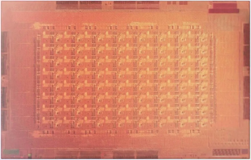
Here is what the MTIA v2 chip looks like:
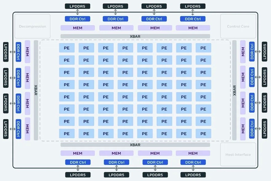
And here is the block diagram of its various units, controllers, caches, and interconnects:
The MTIA v1 chip was etched in the 7 nanometer processes from Taiwan Semiconductor Manufacturing Co and it had an area of 373 mm2 (19.34 by 19.1 mm2); it ran at a mere 800 MHz. With the MTIA v2, the chip is etched using 5 nanometer processes, and Meta cranked up the clock speed by 68.8 percent to 1.35 GHz and made the chip much bigger – 421 mm2 (25.6 mm2 by 16.4 mm2) – so it could jack up the SRAM on the chip. That 12.9 percent increase in area and 68.8 percent increase in clock speed drove up the power consumption by a factor of 2.6X to 90 watts. Sparsity support was added to the PEs and in many cases the resulting performance was driven up by nearly 7X for matrix operations. On the vector cores, SIMD operation performance went up by 72.5 percent, a tad bit better than the clock speed increase.
As with the MTIA v1, the MTIA v2 is an 8 x 8 grid of processing elements, or PEs. With the MTIA v1, those PEs were based on the RISC-V architecture, and one core was designed to deal with scalar work and the other core had vector extensions to do operations on integer and floating point data.
The basic layout of the MTIA v2 is very similar to the MTIA v1. Both have a total of 64 PEs, which are wrapped on all sides with a crossbar fabric that links the PEs to DDR5 memory controllers, four on each side for a total of sixteen memory channels. Meta, like Nvidia with its “Grace” CG100 Arm server CPUs, has opted to use the LPDDR5 memory commonly used in laptops. (The LP is short for low power.) With the MTIA v1, the off-chip LPDDR5 memory weighed in at 64 GB of capacity and 176 GB/sec of bandwidth across those sixteen channels. With the MTIA v2, the capacity is doubled to 128 GB and the memory speed is goosed by 16.4 percent, which boosts the bandwidth by the same amount to 204.8 GB/sec.
Meta has not provided details on the architectural changes it has made inside of the PEs, but it did provide plenty of comparative stats:
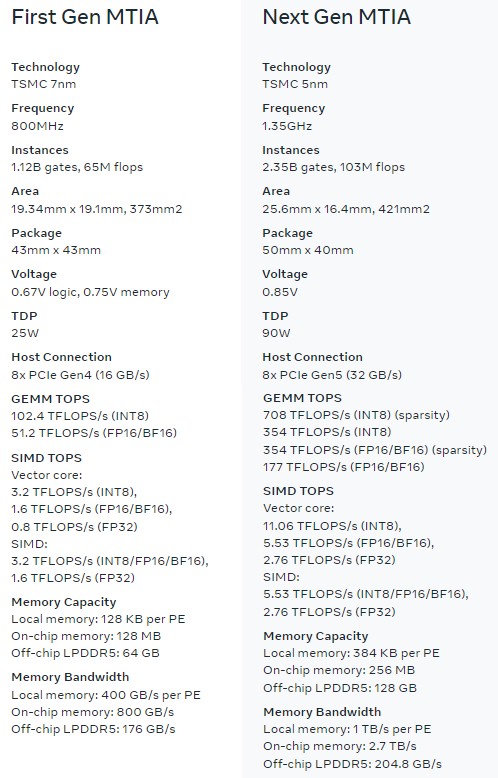
The SRAM memory assigned to each PE in the MTIA v2 has been increased by 3X compared to the MTIA v1, and the shared SRAM memory that spans all 64 cores has been increase by a factor of 2X to 256 MB for the MTIA. Interestingly, the bandwidth on the local memory on each PE has been increased by a factor of 2.5X to 1 TB/sec, and the bandwidth of that shared SRAM memory has been boosted by 3.4X to 2.7 TB/sec.
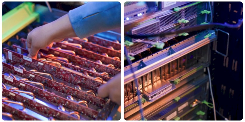
The MTIA v2 has a PCI-Express 5.0 x8 controller with 64 GB/sec of bandwidth to connect to hosts through a PCI-Express switched fabric, and the MTIA v1 had a PCI-Express 4.0 x8 controller with 32 GB/sec of bandwidth. With the MTIA v1 cards, there was one chip per card, but with the MTIA v2, there are two chips per card and they share a physical PCI-Express 5.0 x16 connector to attach to a host. Like this:
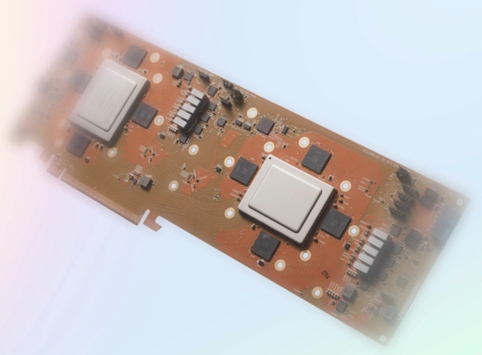
The four black blocks surrounding each MTIA v2 chip are the LPDDR5 memory banks, which are 32 GB each. (Meta made that image look all fuzzy at the edges, we did not.)
Meta is putting a dozen of these cards into a single chassis, for a total of 24 MTIA v2 chips per enclosure; three of these chasses go into a rack for a total of 72 accelerators per rack. PCI-Express 5.0 switching is used to link the accelerators to each other and to hosts within a rack, and there is an option to have the enclosures use a network interface card with RDMA (it could be InfiniBand, but it is probably Ethernet with RoCE). That is 6.5 kilowatts for the accelerators per rack, for just under 50 petaflops of INT8 inference performance on GEMM calculations with sparsity on. (The MTIA v2 is rated at 708 teraops INT with sparsity.)
An Nvidia “Turing” T4 accelerator, weighing in at 70 watts, can do 130 INT8 teraops or 260 INT4 teraops and probably costs around $1,500. An Nvidia “Hopper” H100 can do 4 petaflops at FP8 precision, which is admittedly a lot. But it takes 700 watts to do that and it costs at least $30,000 per H100. The H100 has lots more memory bandwidth, but not as much memory capacity.
The MTIA v2 does 5.5X more INT8 inference work than the T4 for 1.3X more power consumed. The H100 does 5.7X more work, but consumes 7.8X more power and probably costs anywhere from 10X to 15X as much if Meta can make the MTIA v2 cards for somewhere between $2,000 and $3,000, as we expect.
All of this hardware brings us all the way back to the co-design with the Meta software stack, which runs AI inference and training atop the PyTorch framework that it created and open sourced:
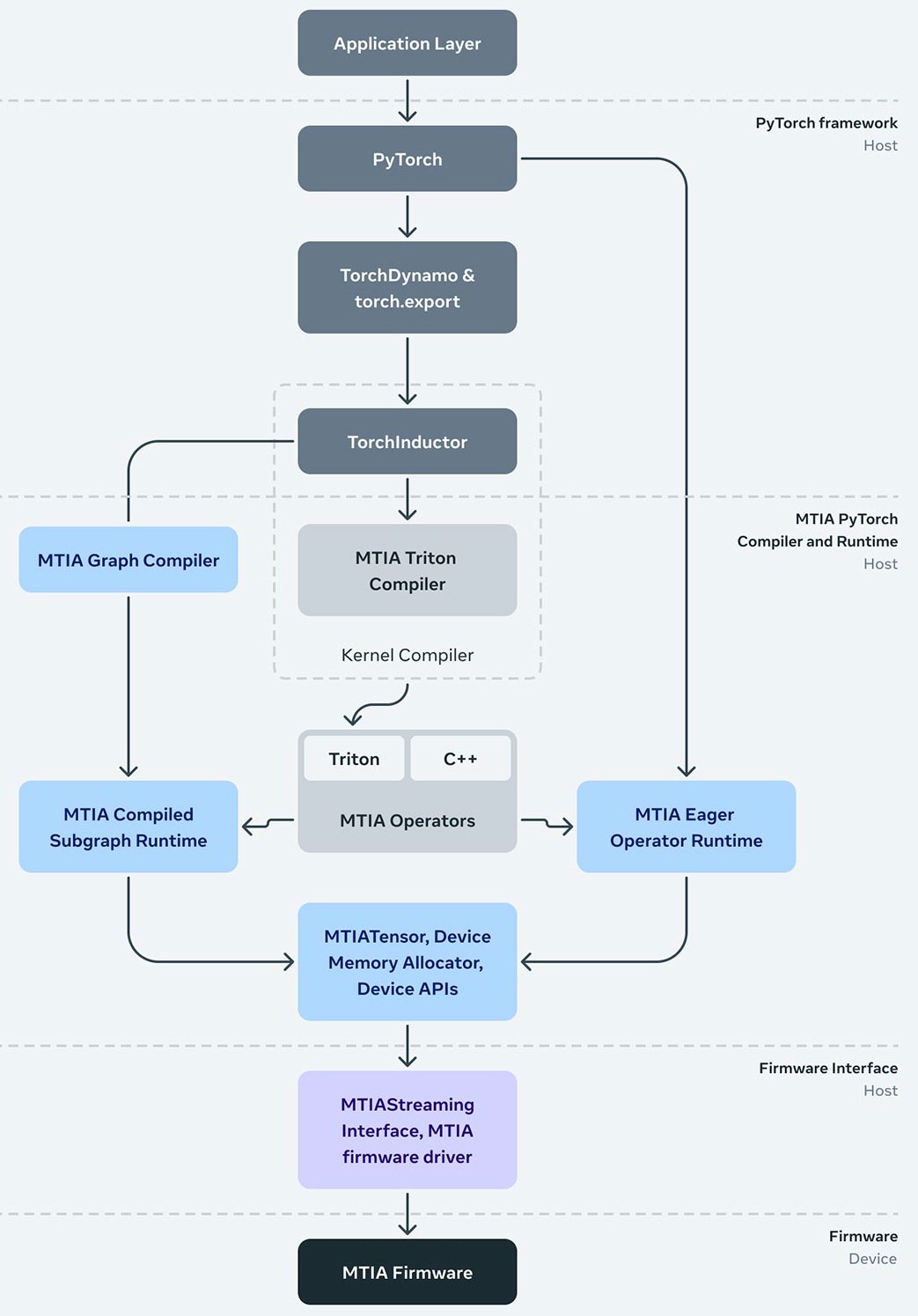
It is interesting that this software stack includes the open source Triton language and compiler – which is not to be confused with Nvidia’s Triton inference server that is part of its AI Enterprise stack. This Triton was created by researchers at Harvard University and IBM back in 2019 and open sourced by OpenAI in 2021 when it was still open for everything but business.
Triton is a Python-like, C-based language for creating machine learning kernels that can get the kind of performance that highly tailored libraries in the Nvidia CUDA stack – which take a lot more effort to create and use – can get on hardware. One of the important things that Meta has done with MTIA is to make sure it is compatible with the Triton language.
We would love to see how a future MTIA chip will be used train models, or tune pretrained models.


Combining AI With HPC To Find Better Battery Designs
The melding of low and high precision mathematics to accelerate the pace of scientific discovery has been a topic of discussion for some time now. During her keynote at ISSC last year, AMD chief executive officer Lisa Su mused that the combo could vastly reduce the energy requirements to scale …
AMD Previews “Turin” Epyc CPUs, Expands Instinct GPU Roadmap
Computex, the annual conference in Taiwan to showcase the island nation’s vast technology business, has been transformed into what amounts to a half-time show for the datacenter IT year. And it is perhaps no accident that the CEOs of both Nvidia and AMD are of Taiwanese descent and in recent …
Meta’s Velox Means Database Performance Is Not Subject To Interpretation
A decade and a half ago, when Dennard scaling ran out of gas and many of us were starting to first think about what the end of Moore’s Law might look like should that day ever come, a bunch of us were kicking around what it might mean. People brought …
Ah, Triton, the cerulean merman cacophonous conch bugler son of that seafaring member of the twelve cheeky Olympians, Poseidon V3 of the Neoverse! A rebel to be sure, mythologically tridented as Triton-C, Triton-IR, and Triton-JIT, with threads like that of marsh frogs. Did v1’s RISC-V PE impudently challenge MTIA v2’s Triton to a contest of musical genAI training, and then drowned architecturally in punishment per Meta’s poetic Virgil Aeneid? Inquisition minds … q^8
Interesting to note that outside of the addition of sparsity to certain datatypes, the efficiency of the MTIA v2 (90W) actually _decreases_ in efficiency as measured in TOPS/Watt vs the MTIA v1 (25W).