

Over the last several years we have seen many new hardware architectures emerge for deep learning training but this year, inference will have its turn in the spotlight. For those chips that can manage to do both sides of the workload on the same device with edge-ready efficiency, a market awaits–albeit an emerging one.
Most devices geared toward convolutional, recurrent, and other large neural networks need relatively big amounts of on-chip memory for storing weights and layers for the long iterative training process. With the datacenter chips that do both training and inference, the same big piece of silicon does the much lighter lifting of inference, which is convenient but not at all efficient.
These shortcomings of memory-laden AI chip architectures have opened the door for neuromorphic devices as well as other approaches to machine learning, including spiking neural networks. The problem is, both neuromorphic devices and spiking nets are far more oriented in research than commercial reality, even if the business case is emerging.
IBM’s True North and Intel’s Loihi are years away from becoming viable neuromorphic hardware products and research efforts like Spinnaker and Neurogrid are more focused on modeling neurons than moving neuromorphic computing to the AI chip front lines. Spiking neural networks have some research traction but to date have none of the same appeal of convolutional, recurrent and other machine learning approaches. Loihi is a promising architecture in terms of its capability, efficiency, and manufacturability but is still on the horizon, leaving early room in an early market.
This presented an opportunity for Brainchip, a company that has just released preliminary details of its neuromorphic architecture for spiking neural networks that takes aim at both datacenter and edge, training and inference, and for markets including computer vision, financial tech, and cybersecurity. The company makes a clear case for the burdened state of current AI chips in terms of efficiency and shows how spiking nets could capture some of the mainstream interest given software tooling to make the convolutions to spike transition easier.
On first sight, it all might sound too esoteric and research-rooted for real productization. But digging a little deeper, it could be the company, founded in 2013 by ex-FPGA and machine learning security backgrounders, is onto something with market potential. We fully expect this will not be the only silicon delivered focused on SNNs with a type of neuromorphic architecture, but it is the first—assuming all goes according to schedule. And that is hard to say while the company is in patent pending mode with no process technology selected.
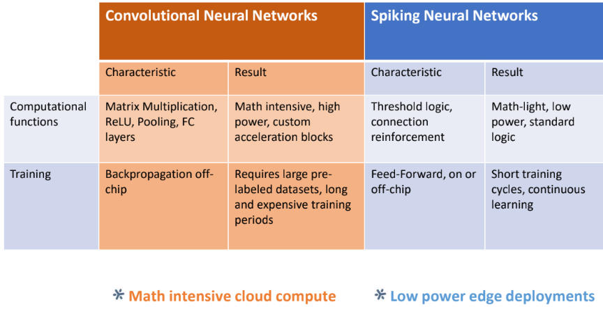 Power is always a factor but in inference at edge, consumption in the sub-five watt range is required. Brainchip’s assertion is that the back propagation, iterative CNN process creates too much overhead. The idea is to send data through the network for training, setting the synaptic weights and neuron firing threshold in advance and switch into inference mode using that much smaller data in much more compact memory per unit of compute. No HBM, no MAC units—no power overhead.
The reason goes back to the above statement about the way deep learning training and inference chips have to load up on expensive (power and otherwise) memory to capture network layers and weights. Even with quantization and paring, there is no way around this and in fact, as networks get more complex from training, inference becomes slower and less efficient.
Brainchip’s claim is that while a convolutional approach is more akin to modeling the neuron as a large filter with weights, the iterative linear algebra matrix multiplication on data within an activation layer and associated memory and MAC units yields a power hungrier chip. Instead of this convolutional approach, an SNN models the neuron function with synapses and neurons with spikes between the neurons. The networks learn through reinforcement and inhibition of these spikes (repeating spikes are reinforcement).
The ability to change the firing threshold of the neuron itself and the sensitivity to those spikes is a different and more efficient way to train, albeit within complexity limitations. This means way less memory (there are 6MB per neural core) and a more efficient end result.
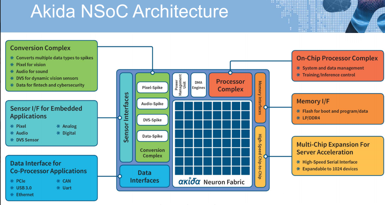
The “Akida” device has an on-chip processor complex for system and data management and is also used to tell the neuron fabric (more on that in a moment) to be in training or inference modes. This is a matter of setting the thresholds in the neuron fabric. The real key is the data to spike converter, however, especially in areas like computer vision where pixel data needs to be transformed into spikes. This is not a computationally expensive problem from an efficiency perspective, but it does add some compiler and software footwork. There are audio, pixel, and fintech converters for now with their own dedicated place on-chip.
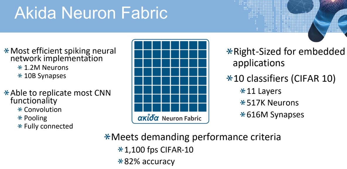
The PCIe links allow for datacenter deployments and can scale with the multi-chip expansion port, which is a basic high speed serial interface to send spikes to different neural processing cores—expandable to 1024 devices for very large spiking neural networks. The Akida neuron fabric shown below has its own 6MB on-chip memory and the ability to interface with flash and DDR.
“If you want a self-contained network on chip, you can store in flash and not external DRAM. If you want a more complex network that, say, processes the first 11 layers, stores it, then repeats with next layers, you can also do that in a time division multiplex manner,” Beachler adds.
As one might image, Brainchip can’t tell us what’s inside those little neural processing cores or what makes them neural exactly. To be fair, however, the “neural” part of the story is really about the network model anyway. Still, each of these cores can emulate neurons and synapses and each is interconnected with an on-chip bus for global connectivity so spikes coming out of one neuron core can go to any other core or to other chips via the expansion port.
“A lot of research has gone into the neural processing cores and fabric,” Beachler says. “We have experience with many different types of spiking models and have an optimized implementation but the patents have not been granted. I can say that we can do this in a low die size with a high neuron count—it will have 1.2 million neurons and 10 billion synapses.”
There are no mainstream frameworks for SNNs so Brainchip had to roll their own. In essence, it does not look much different than a CNN framework but the key is in the conversion. For instance, the company’s SNN processor does not work directly with image data, rather a pixel to spike converter handles the transition. This strikes us as one of those “devil in the details” moments we’ve experienced with all of the AI chip startups we have dug into. The architecture and stack looks right but the compiler (and in this case, converter) has some seriously heavy lifting to do behind the scenes that gets especially complex when users step out of the zone of defined neural network frameworks.
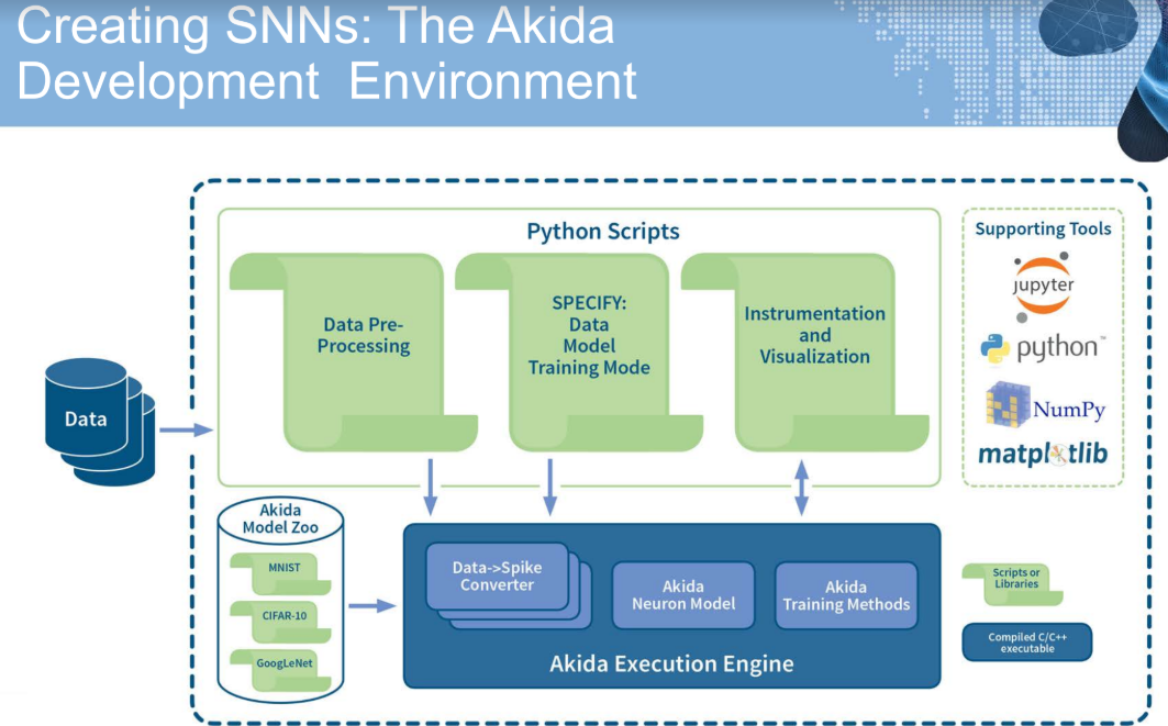
The development environment looks similar to any machine learning framework. Users describe their SNN model which is stored in the model zoo. The chip will come with three pre-created models (CIFAR, Imagenet and MNIST) or they can create their own architecture. A Python script can be used to specify data location, model type, and this is shipped off to the Akida execution engine with the Akida neuron model and training methodology with conversions (from pixel to spikes, etc.). It goes into training mode or inference mode depending on user settings.
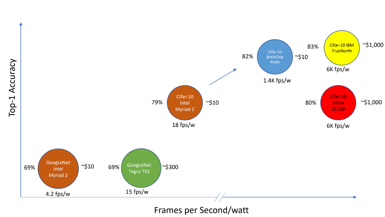
Even though silicon is expected this year, Brainchip has still not set on which process technology to use yet. Beachler tells The Next Platform that they are evaluating both 28nm and 14nm as options but of course, the smaller they go, the more expensive the whole proposition becomes. “For our users and especially in embedded, the targeted price point needs to be under $20 to run in any volume and we’re targeting below that. We are finishing the layout of the device and we are aiming not for hundreds of dollars of chip, but tens.” For perspective, Intel’s Loihi is 14nm process and has 131,072 neurons and 130 million synapses but with the process technology it is hard to say potential pricing.
The CIFAR 10 benchmark they are rating their performance and efficiency on isn’t common but the chart below highlights more than just an apples to apples comparison. It shows that the other neuromorphic architecture here, True North, has great performance and efficiency but is expensive given the process technology and while Intel’s “Loihi” is not shown, it is likely in that same camp. The real story for Brainchip is the price for relative accuracy and for more inference shops, a 10% difference can be a big deal, according to Beachler.
Brainchip’s “Akida” chip is aimed at both datacenter and training and inference but realistically, as the company’s head of product, Bob Beachler tells us, inference at the edge is the prime target. This includes vision systems in particular but also financial tech applications where users cannot tolerate intermittent connectivity or latency from cloud.
The company’s Akida Development Environment will be released in Q3 of this year with the FPGA based accelerator available at the end of 2018. By 2019 the company want to roll out its SoC samples with the Akida Acceleration Card available at the end of 2019 with an undisclosed number of chips per board.
Being the first to market with a device like this is no guarantee of success but it does pave the way for conversations we expect to have during the rest of 2018 about neuromorphic devices moving somewhat more into the mainstream and certainly the relative benefits of spiking neural networks for at least some edge workloads. As for the datacenter-scale side of this story it remains to be seen. Most startups we are talking to are pitching us tales of chips that do double duty in the datacenter and at the edge, the better stories are those where it does both training and inference in each, but the best story is when it’s clear one single architecture can fit all bills expertly. That one is being told but not played out…at least not yet.

On the Fringes of Useful Neuromorphic Scalability
When it comes to novel computing architectures, whether in quantum, deep learning, or neuromorphic, it can be tricky to get a handle on how incremental improvements in processor counts translate to real world improvements since these bumps in element counts often don’t have perfect parallels to CPUs or even GPUs. …
How AWS Can Undercut Nvidia With Homegrown AI Compute Engines
Amazon Web Services may not be the first of the hyperscalers and cloud builders to create its own custom compute engines, but it has been hot on the heels of Google, which started using its homegrown TPU accelerators for AI workloads in 2015. AWS started with “Nitro” DPUs in 2017 …
Lenovo Bundles VMware Stack At The Edge
Enterprises and tech vendors alike for the past few years have been talking about the growing importance of the edge in the increasingly distributed IT environment. It’s at the edge where more data is being generated and stored, and organizations are feeling the need to process, analyze and act on …
This is meaningless since its not comparing its results with state-of-the-art architectures: ResNet, Inception v4, DenseNet, NASNet, etc. It could even have done a comparison with SqueezeNet which is smaller and computationally more efficient.
I did (as said in the article) think using CIFAR 10 was a little out there. There is no way to do a real apples to apples with this device against anything else out there so far really.
I guess even more complex network model will match to the real field application. But the most basically principle will not be different from the CIFar-10. So they use a simple model to make comprearation is not a bad idea. The unhappy thing I feel is the 82% accacy . Also they did not tell the bottom architecture is pure digital , or analog Mixed signal or even new type nano device?
For me at least, the important thing here is the advancement of special-purpose (and event-driven, hence power efficient) neuromorphic hardware. Sure, we have powerful GPU-inspired architectures and they certainly have their place in high-performance general-purpose computing, but now we’re seeing potential products being developed inspired by real nervous systems (and likely researched using simulations on GPU-based high-performance system) and will hopefully serve as excellent widely available experimental platforms. This in my mind will accelerate the research and development of a low-power requirement (and hence mobile) intelligent ability for machines. Don’t forget that we’re still discovering much about single neuron function, let alone the entire anterior nervous system itself, and all of this will inform the function of our hardware implementation. Fascinating times ahead!
The bottom design of synapse is pure digital, or analog&mixed signal or memristor ?
It’s pure digital, the chip is currently in production.