

In the first story of this series, we discussed the Infinity fabric that is at the heart of the new “Naples” Epyc processor from AMD, and how this modified and extended HyperTransport interconnect glues together the cores, dies, and sockets based on Eypc processors into a unified system.
In this follow-on story, we will expand out from the Epyc processor design to the basic feeds and speeds of the system components based on this chip and then take a look at some of the systems that AMD and its partners were showing off at the Epyc launch a few weeks ago.
Let’s start with the basic “Zeppelin” chip building block and work our way out to the systems.
AMD designed the Zeppelin die to support both a performant 1S desktop MCM and as a performant building block for a scalable multi-die server MCM architecture. AMD calls the nominal amount of additional logic required to implement a multi-die packaging strategy the “server controller hub” as shown in the figure below:
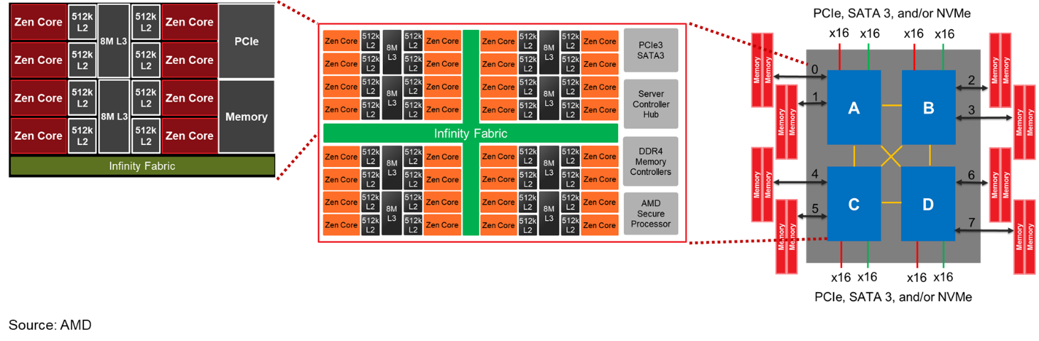
Epyc will initially ship with four Zeppelin die in a multi-chip module (MCM), supporting 8, 16, 24, and 32-core variants (using 2, 4, 6, and 8 active cores per die) with identical memory and I/O features.
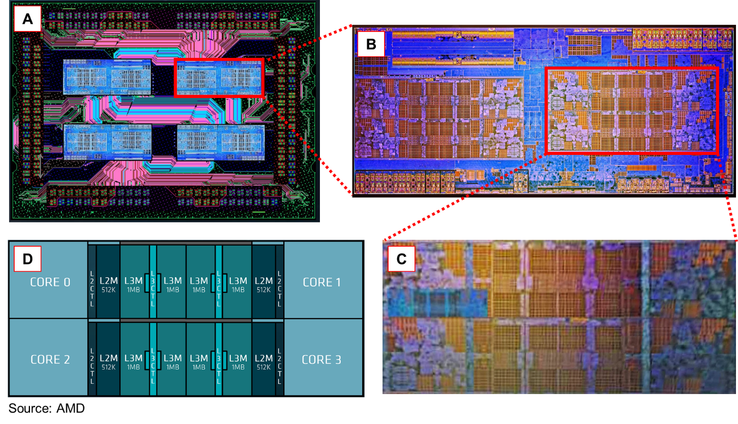
The figure above decomposes an Epyc MCM into Zeppelin die and Zen quad-core complexes:
- Composite of Epyc MCM schematic diagram and four Zeppelin die photos
- Zeppelin die close-up showing two Zen quad-core complexes
- Zen quad-core complex close-up
- Zen quad-core complex block diagram
Each Zen core (two hardware threads, AMD’s Zen core architecture is multi-threaded) contains a 512 KB of L2 cache. All four of the cores in a quad-core complex have access to shared 8MB L3 cache dedicated to the quad-core complex. That yields a total of four cores and eight threads per quad-core complex. There are two quad-core complexes on a Zeppelin die. An Epyc MCM might therefore have as much as 16 MB of L2 cache (depending on how many cores are active) and will have an aggregate total of 64 MB of L3 cache. There is a balance of one memory controller per each Zen quad-core complex in the Zeppelin SoC architecture.
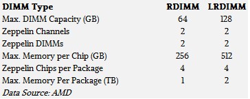
Each Zeppelin die integrates two DDR4 memory controllers, each capable of driving four DIMM banks in two slots with ECC at up to 2.67 GHz. Each DIMM slot can support up to 64 GB RDMIMMs or 128 GB LRDIMMs, for a total of 1 TB of RDIMM and 2 TB of LRDIMM memory per Epyc MCM.
In a two-socket configuration, system memory capacity doubles to 2 TB of RDIMM or 4 TB of LRDIMM memory, but system I/O is identical to a one socket machine– half of the I/O lanes are used for the Infinity Fabric links between the two SoC sockets (described in the prior story).
AMD’s Epyc architecture uses Infinity Fabric to form closely knit, non-uniform memory architecture (NUMA) clusters between Zeppelin dies on-chip and across sockets within a two-socket server node. This is the same class of NUMA topologies that enabled AMD’s Opteron processors to perform so well in machines with two, four, and eight sockets in the past, but with far greater interconnect bandwidth, lower latency, and added flexibility.
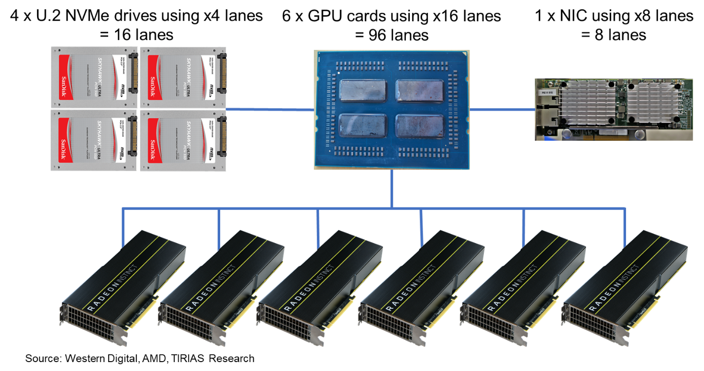
Each Zeppelin die also integrates 32 PCI-Express 3.0 lanes, configurable in pairs, and thus the Epyc MCM supports up to 128 PCI-Express lanes in total. The configuration of Epyc’s PCI-Express 3.0 pairs as NVM-Express, SATA, or socket-to-socket Infinity Fabric is determined when the motherboard is designed. An Epyc MCM can directly connect up to 32 SATA or NVM-Express devices.
The Epyc one socket GPU accelerated node shown below has eight remaining unallocated PCI-Express lanes. As Epyc is a fully bootable MCM, the remaining PCI-Express lanes could be used for more storage, another NIC, and so forth.
AMD designed Zeppelin’s MCA to fully communicate performance and error states to the control fabric. Not all this data will be used for system management in initial Epyc implementations, because there are many system behaviors that can be governed in Zeppelin that system designers do not have available today. As Epyc enters the market, it will enable system reliability management in scale-out servers that is simply not available today outside of purpose-designed high availability systems.
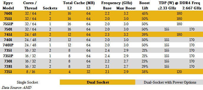
The Epyc chip can also sense when a workload that is using all its cores is not latency sensitive – it can then slow the clock rate for all the cores to reduce the aggregate core idle time and save power. Epyc also has enough detailed knowledge of its own silicon operating conditions that its fine-grain real-time control enables system operators to select power limits for performance per watt trade-offs as a boot-time configuration option. For example, an Epyc SoC qualified to run at a 155 watt thermal design power (TDP) can be set as low as 140 watts and as high as 175 watts. See the table and figure below for more examples.
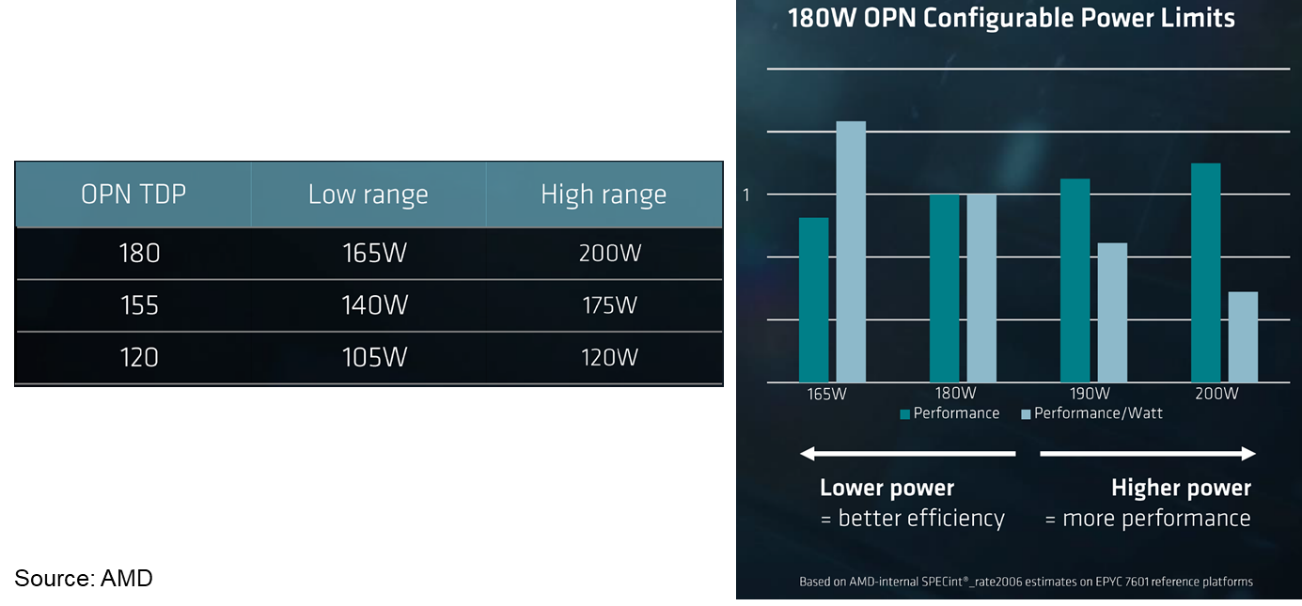
We estimate that AMD budgeted about 25 watts for the “uncore” parts of the Zeppelin chip – that is, the memory controller, I/O, Infinity Fabric, management, and other components outside of the cores and memory controllers, or about 100 watts across the four Zeppelin dies in an Epyc MCM, plus about 5 watts for each active Epyc core pair (with variance due to memory speed, processor speed, binning, and other factors). That matches eight cores at 120 watts and 32 cores at 180 watts TDP.
This power consumption split also demonstrates that research and development to reduce core power consumption even lower will be subject to diminishing returns, as non-core functions of AMD’s Zeppelin die now consume more power than all the processor cores combined. It also shows that AMD and Nvidia are focusing their R&D investments in the right place as they weigh power per bit transmitted between dies against architectural innovation and manufacturing costs. (We discussed multichip implementations from Intel and Nvidia in the prior story.)
Semiconductor Economics 101
There are only a few key rules to manufacturing processors in volume and earning a good margin while doing so:
- Keep the die small. Wafer defects are random and spread across each die, so the chances of a manufacturing defect rise as area increases. Large processor dies tend to produce expensive processors because they are expensive to manufacture due to lower yields. You throw a lot away.
- Known good dies are easy to package. Dies that survive test and validation can be just as easily packaged singly or in multi-chip packaging, it does not really make a difference. There is very little fallout from damaged dies during packaging these days. MCMs are more expensive to manufacture than single-chip packages, but better die yields should lower die costs to the point that MCMs have lower overall costs.
- As manufacturing volume increases, pricing decreases. This is true for almost every manufacturing operation, not just semiconductors, which includes MCM manufacturing.
AMD effectively changed the rules for designing large core count processors like Epyc, using Infinity Fabric and Zeppelin building blocks. This design takes AMD out of the game of trying to out-manufacture Intel (or anyone else) at aggressive die sizes while using commercial foundries such as GlobalFoundries. Using several smaller dies in the same MCM has better defect density economics, while also harnessing much more aggregate silicon area (and therefore much higher transistor counts and more complex feature sets) than can fit inside the largest reticle size.
AMD can use the same Zeppelin building block to create a complete product stack with a variety of design points. Part of that architectural choice was to create flexible SERDES links that customers can configure with each motherboard design for Infinity Fabric, PCI-Express, SATA, and NVM-Express links.
The Zeppelin die is used across AMD’s Epyc data center products and Ryzen desktop products. AMD’s back-end production process at GlobalFoundries first sorts Zeppelin wafers based on defect densities. Wafers with the lowest defect densities and several other beneficial characteristics are separated for Epyc and Ryzen Pro use and run through a more rigorous back-end manufacturing, verification, and validation process than wafers destined for Ryzen consumer products. Also, a few commercial features are disabled for consumer products.
The aggregate volume of die used to create multiple product stacks based on the same building block also contributes to driving the volume of that die up and the price down. Using several small die in many different products acts as a force multiplier for volume pricing.
Epyc Ecosystem Support
As fun as technical detail is (and for us it is fun), the best part of AMD’s Epyc launch was the breadth, depth, and coordination with AMD’s customers and ecosystem.
Baidu and Microsoft anchored AMD’s launch keynote with messages about using Epyc in their cloud infrastructure, with Microsoft promoting its Open Compute Project (OCP) Project Olympus rack and server standards. Microsoft stated that they had enabled and optimized Windows Server 2016 for Epyc as of the keynote, and that Azure would deploy Epyc by the end of 2017. Dell EMC and HPE also showed Epyc servers onstage.

AMD listed these customers as actively working to bring Epyc-based servers to market (in order of appearance on AMD’s slide):
- HPE – Hewlett Packard Enterprise
- Inventec –Taiwanese original equipment manufacturer (OEM)
- H3C – Chinese data center networking equipment spin-off from Huawei and HPE China
- Tyan –Taiwanese data center original design manufacturer (ODM)
- Dell EMC – Data center division of US-based Dell Technologies
- Lenovo – Chinese OEM that bought IBM’s PC and x86 server businesses
- Gigabyte – Taiwanese consumer and commercial ODM and OEM
- Supermicro – US-based data center OEM and ODM
- Microsoft – US-based cloud operator defining OCP hardware standards
- Sugon – Chinese data center OEM, was Dawning Information Industry
- ASUS – Taiwanese consumer and commercial ODM
- [not listed, perhaps a last-minute addition] Wistron – Taiwanese ODM group that includes Wiwynn, a cloud data center ODM brand
ASUS, Gigabyte, and Tyan also sell server motherboards under their ODM businesses, in addition to server chassis. Dell EMC did not open its Epyc server chassis, but did speak generically about Epyc contributing to Dell EMC’s PowerEdge brand attributes and focused on data center security. Tyan did not open its server chassis either, but showed comprehensive specifications for its Epyc servers. H3C and Lenovo did not participate in Epyc launch activities.
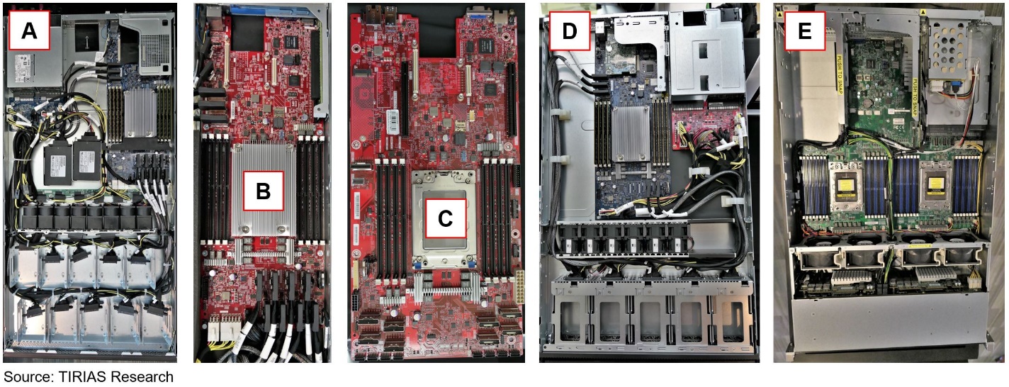
It looks like there is only one way to fit two Epyc sockets and 32 DIMMs into a standard width server chassis, while leaving space for the rest of the components, as shown in Figure 12.
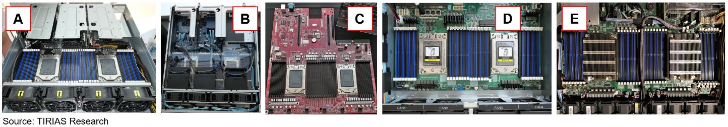
Several vendors unveiled their own variants of AMD’s reference motherboard in ready-to-ship 2S/2U chassis configurations, as shown above:
- ASUS RS720A-E9
- Gigabyte R281-Z92
- Inventec K885G4
- Sugon A620-G30
- Supermicro AS-2023US-TR4
The ASUS, Gigabyte and Supermicro 2S systems all support 24 2.5-inch U.2 NVM-Express drives, while the Inventec system supports 24 2.5-inch SAS3 drives and the Sugon system opts for 32 2.5-inch SATA drives. Supermicro said that this Epyc server is their “best 2S server ever” and it is already shipping.
Four vendors showed PCIe GPU-accelerated servers, two of them 2S servers and two of them 1S servers, as shown in the figure below:
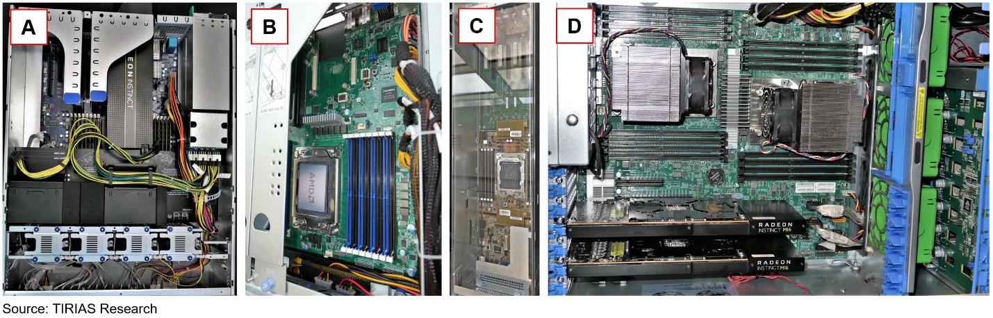
Here is what is outlined in the figure above:
- Gigabyte G220-001 – 2S/2U with two x16 GPU slots
- Inventec P45G4 – 1S/1U with four x16 GPU slots
- Wistron H421G23-P08 – half-width 1S/4U with four x16 GPU slots, for eight GPUs per 4U of rack height
- Supermicro AS-4023S-TR – 2S/4U tower with two x16 GPU slots
Hewlett Packard Enterprise announced its aggressively dense, Epyc-based 1S/1U Cloudline CL3150 cloud storage server onstage during the keynote. Available in August, the CL3150 is an OCP design (it does not appear to be Project Olympus compatible) that uses OCP’s mezzanine slot for OCP-compliant NICs. In the demo area, Wistron showed a less dense 1S/1U cloud storage server and Supermicro showed a more traditional hyperconverged compute plus storage form factor, as shown in the figure below:
These machines include:
- HPE Cloudline CL3150 1S/1U system with 24 U.2 2.5-inch NVM-Express bay
- HPE Cloudline CL3150 1S motherboard
- Wistron S111G20/G23-U10 1S motherboard
- Wistron S111G20/G23-U10 1S/1U system with 10 U.2 2.5-inch NVM-Express bay
- Supermicro AS-2123US-TN24R25 2S/2U system with 25 U.2 2.5-inch NVM-Express bays
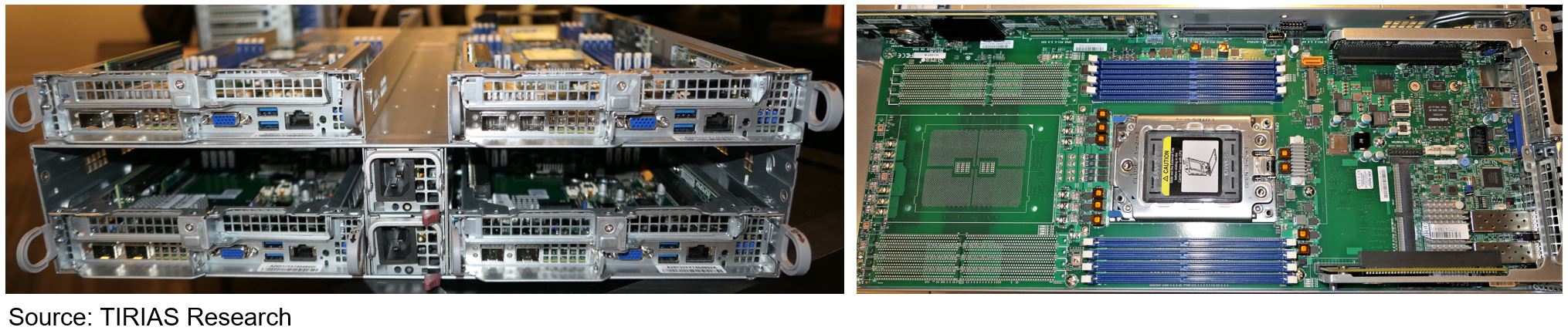
Supermicro’s AS-2123BT-HNCOR high density form factor, shown below, fits four 1S or 2S sleds into a 2U vanity-free rack chassis (left photo). Sleds can be configured as fully populated with two Epyc processors and their memory systems or they can be built with only one Epyc socket populated to save costs (right photo).
Adding It All Up
The net effect of all the Epyc launch day demonstrations is that AMD did an outstanding job of lining up customer and software partner support (not discussed here for brevity) ahead of the Epyc launch. AMD’s hardware demonstrations spanned a wide gamut of design and cost points. Plus, we talked with all of AMD’s customers who were at the event, and all of them are honestly excited about shipping AMD-based systems. We have not seen this level of customer support since AMD’s Dual-Core Opteron launch in 2005.
Mark Papermaster was not exaggerating when he stated that AMD had gone back to a clean whiteboard at the start of Epyc’s design cycle five years ago. AMD’s Epyc architecture is different than monolithic processor architectures, and in quite a few ways it is superior.
AMD’s next challenge is to execute on its Epyc volume ramp this fall. After that, the company will need to sustain their product innovation to stay ahead of Intel. But, first things first. Epyc launch day was a great day for AMD and a great day for the global server market.
Paul Teich is an incorrigible technologist and a principal analyst at TIRIAS Research, covering clouds, data analysis, the Internet of Things and at-scale user experience. He is also a contributor to Forbes/Tech. Teich was previously CTO and senior analyst for Moor Insights & Strategy. For three decade, Teich immersed himself in IT design, development and marketing, including two decades at AMD in product marketing and management roles, finishing as a Marketing Fellow. Paul holds 12 US patents and earned a BSCS from Texas A&M and an MS in Technology Commercialization from the University of Texas McCombs School.

Other Than Nvidia, Who Will Use Arm’s Neoverse V2 Core?
We are still plowing through the many, many presentions from the Hot Interconnects, Hot Chips, Google Cloud Next, and Meta Networking @ Scale conferences that all happened recently and at essentially the same time. And we intend to take our usual, methodical approach of finding the interesting bits and doing …
Cisco: Datacenter Demand Strong, Supply Not So Much
The good news, and we all need to be looking at the bright sides of things a bit these days is that the biggest IT shops in the world want to buy a lot of datacenter gear from Cisco Systems. Across the board with large enterprise and commercial accounts, the …
Details Emerge On Nvidia’s “Grace” Arm CPU
Imagine, if you will, that Nvidia had launched its forthcoming “Grace” Arm server CPU three years ago instead of early next year. How much better would Nvidia be fairing in the gaming and cryptocurrency downdraft that is impacting its sales today? Sometimes, little changes make a big difference in the …
Diagram 1 shows an infinity interconnect path between dies B and C, as does diagram 4 of your 20th June article and some other AMD diagrams. However, image A in diagram 2 does not have any visible tracks for this, while all the other five paths are clearly visible.
(Thanks for your HPC coverage in general, and especially of the Phi, Xeon and Epyc CPUs!)