Hewlett Packard Enterprise is not just a manufacturer that takes components from Intel and assembles them into systems. The company also has a heritage of innovating, and it was showing off its new datacenter architecture research and development testbed, dubbed The Machine, as 2016 came to a close.
While The Machine had originally attracted considerable attention as a vehicle for HPE to commercialize memristors, it is a much broader architectural testbed. This first generation of hardware can use any standard DDR4 DIMM-based memories, volatile or non-volatile. And while large, non-volatile memory pools are interesting research targets, HPE realizes that it has to create a sophisticated interconnect architecture to enable these new memory technologies and systems for commercial deployments at scale and at volume.
The Next Platform has covered the potential of The Machine in the HPC market, and has drilled down into the architectural features of the concept machine and the intertwining of memory and performance in that architecture, but this story will examine the hardware in the actual prototype.
The Machine at HPE Discover London 2016
Instead of showing slides, as it did at Discover 2014, or 3D printed mechanical airflow mock-ups, as it did at Discover 2015 and at Discover Las Vegas 2016, as last year came to a close HPE displayed fully populated boards mounted on production Apollo 6000 series sleds at Discover London 2016. The Machine’s global memory plus processor node design took more physical space than planned 18 months ago, so the sleds were expanded to stick out six inches in front and six inches behind the Apollo 6000 chassis and rack. Because this R&D testbed is not destined to be a shipping product, the extra-long sleds are not much of an operational challenge.
HPE used this relaxed philosophy throughout The Machine’s design – nothing is fully optimized and the designers made many architectural choices in favor of simultaneously learning about multiple aspects of system behavior. The Machine’s modular design allows for different subsystems – memory, storage, network, and compute – to be switched or upgraded separately, so that one component’s cadence does not impede researchers from examining the latest technologies or products for other components.
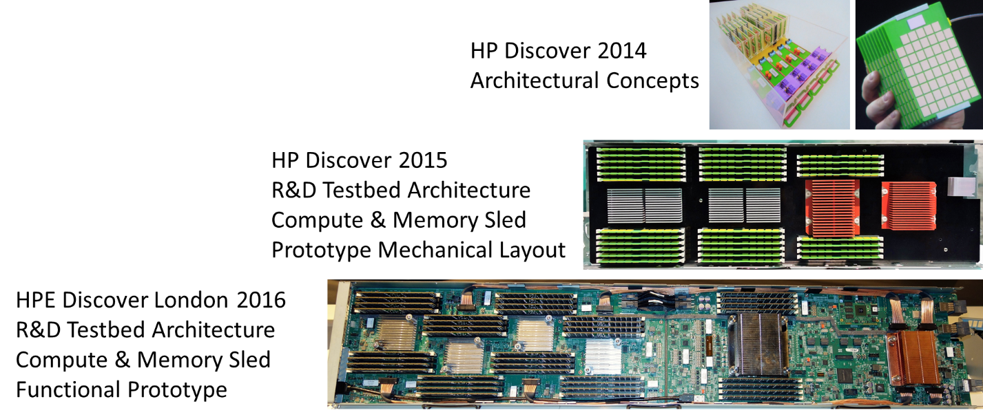
It is apparent from the progression outlined above that HPE researchers were not able to achieve the component packing density they had originally hoped. It is also apparent that did not bother them, as The Machine is an R&D testbed and not headed for production. If this design was destined for production, HPE would invest in integrating much of the logic taking up the extra board space, but since this is a R&D prototype, HPE opted to use off-the-shelf components and rapid prototyping methods wherever possible to balance schedule and performance goals. The result is a mix of copper and fiber cabling with fewer motherboard traces than would have been implemented in a production system. The result is that The Machine’s prototype compute plus memory sled is much too long to fit neatly into its host HPE Apollo 6000 series rack.
In addition to the size, there are mechanical changes from the original mechanical mockups. The mechanical mockups had six DIMM slots per memory fabric interface, where the fully realized design bumps up to eight slots, placing more emphasis on the global memory subsystem. There are many components between the fabric sled switch and the ARM workload processor, and between the ARM workload processor and the global memory pool. The global memory plus compute sled uses two motherboards, as well – one for the sled fabric switch and workload specific system-on-chip (SoC) and the other holds the global system memory portion of the node.
As mentioned above, the 4U chassis were borrowed from HPE’s Apollo 6000 high performance computing design. For The Machine’s R&D testbed, each memory slot on a sled is assigned a unique number, each sled is numbered and each chassis is numbered. That means processor sockets can be referenced by a unique combination of chassis and sled number, and memory slots add the slot number on each sled.
We estimate The Machine’s R&D testbed consumes 24 kW to 36 kW of power. This is a lot for a normal IT data center today, but it is not out of range for current advanced cloud analytics and high performance computing (HPC) deployments.
The Fabric Sled Switch
Looking at The Machine’s node design, from right to left in the bottom photo in the figure above, there are two fabric interconnects on the right side of the board, as well as a management and power interconnect (at the bottom right).
The photo below is a close-up of the right end of the board. The chip under the copper heat sink is the fabric sled switch. The fabric sled switch connects both the global system memory and the workload SoC to the fabric chassis switches. There are four fabric chassis switches and each fabric sled switch connects directly to all four fabric chassis switches (see below for more on the fabric chassis switches).
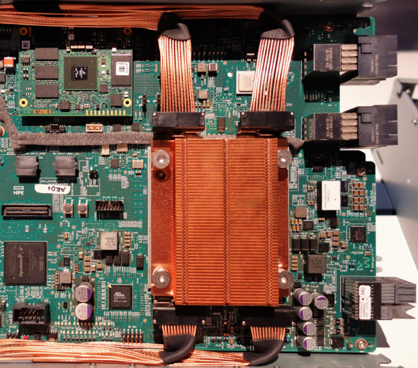
The sled fabric switch connects to the workload SoC through its common motherboard. The memory fabric switches are on a different board planar; running the high-speed interconnect over the top via dedicated cables is not a production-oriented design approach, but acceptable for an R&D prototype.
The Global Memory Pool
The four groups of parallel copper wires directly connect the sled fabric switch to each of the four memory fabric interfaces on the memory portion of the node. These interfaces are rapidly converging on Gen Z – HPE’s work in defining these interfaces is a core piece of its contribution to the Gen-Z consortium. Gen Z’s initial specification supports up to 56 gigatransfers per second (GT/sec) at up to 256 lanes per link) with sub-100 nanoseconds load-to-use memory latencies. For comparison, the PCI Express 4.0 specification’s 16 GT/sec maximum is the minimum spec for Gen Z.
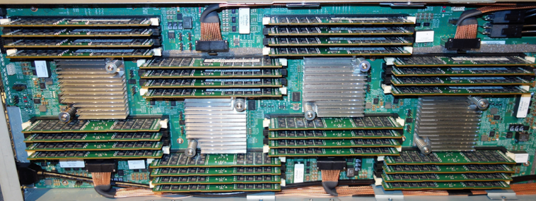
The photo above is a close-up of the four fabric memory interfaces, each with eight DIMM slots. Memory is addressed by a simple scheme using socket, slot, and enclosure numbers for a single, global flat address space spanning directly connected chassis.
Using 32 GB RDIMMs, each fabric memory interface addresses 256 GB of memory, and the four together total 1 TB of memory. There are ten sleds per chassis, for a total of 10 TB of global memory per each 4U of rack height. Eight chassis requires 32U of rack height (leaving room for other switches and power delivery in a nominal 42U rack) and contain 82 TB of globally addressed memory. The table below shows more detail for The Machine memory configurations:

The Processor Node
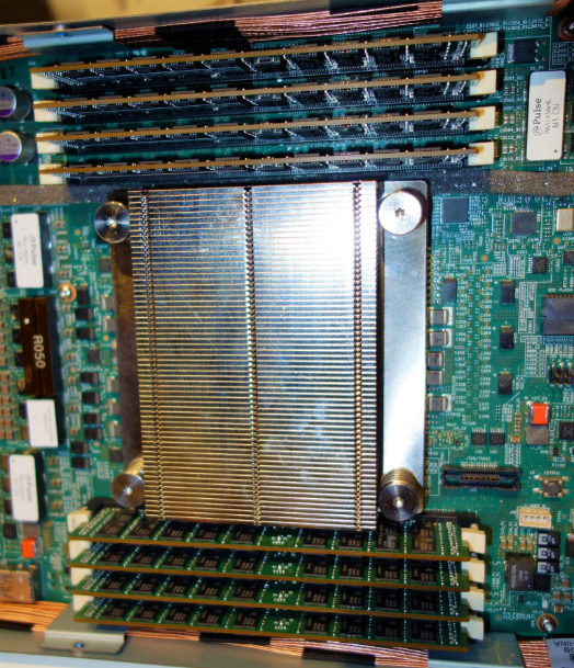
In the figure below you can see the ARM-based workload processor’s heat sink and eight attached DIMM slots. HPE is not yet divulging whose ARM SoC it designed into The Machine’s initial sled design. The workload processor’s memory slots are not globally addressable, they are working memory for the workload processor only. With the same 32 GB RDIMMs, each workload processor has direct access to 256 GB of memory. At one workload processor per sled, that’s 2.6 TB of processor attached memory per 4U chassis and 20 TB of processor attached memory per rack, which brings the total memory per rack to 102 TB.
Does The Machine’s workload processor have to be ARM-based? HPE Labs says no, and adds that The Machine is intended to explore how data-centric architecture impacts code optimization for various processor and coprocessor architectures, including APUs, GPUs, FPGAs, and perhaps hardware accelerators. HPE chose the ARM architecture for this first design iteration to learn about enterprise-grade ARM and ARM’s rapidly maturing server software development ecosystem – a benefit of the above mentioned philosophy of simultaneously learning about multiple aspects of system behavior. However, HPE is looking forward to many new server workload SoC design choices in late 2017 and into 2018.
Gen Z looks like PCIe to the processor, so software developers don’t need to do anything differently to access system resources across Gen Z.
Non-Volatile Memory
HPE has a deep R&D collaboration with Western Digital to develop next generation memory technologies and architecture. However, The Machine is flexible. For example, HPE might decide to outfit global memory with non-volatile DIMM (NVDIMM) and workload processor memory with standard RDIMMs for faster local processing.
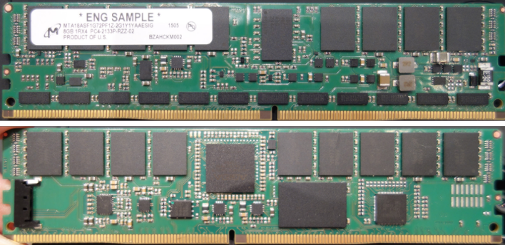
In the photo below, HPE showed off an engineering sample of an NVDIMM based on Micron non-volatile memory chips using a standard DDR4 memory bus, so it can be used in The Machine. (Intel will sell its 3D XPoint non-volatile memory technology developed jointly with Micron under the Optane brand name.) While HPE is simulating non-volatile memory systems today simply by not turning the systems off, HPE Labs will consider switching The Machine over to Optane DIMMs when production quantities of are available on the market. However, using Optane DIMMs will also be predicated on either Intel offering DDR4-compatible Optane DIMMs or Intel opening the Optane interface specifications to third parties. Using Optane NVDIMMs, all the memory capacities mentioned above will still apply to The Machine’s R&D testbed, but it will be a completely non-volatile memory system.
The Network Backplane
The Machine’s compute plus global memory sleds each plug directly into two backplane fabric switches via board connectors on both the sled and the backplane switches. This is shown in the photo below, with two independent and redundant switch boards in the back of each 4U chassis:
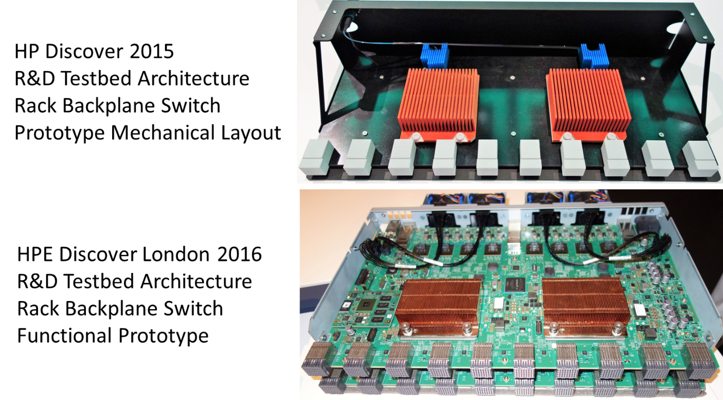
Boards plug in vertically, so that yields ten boards in a 4U height, with the signal boards at the bottom and separate power distribution and management plane connecting at the top.
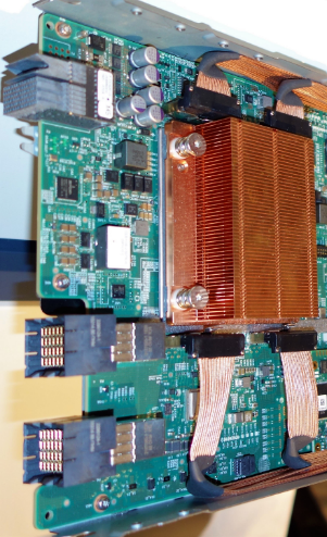
In the photo below, you can see the back of the sled and its matching connectors. Each of the two sled backplane connectors contains two 100 Gb/sec bidirectional copper links between sled and fabric switch. There is no mid-plane and no cabling between the sled and switches, only the multi-lane high-speed board connectors.
There are eight VCSEL electrical-to-optical transceiver modules on each fabric switch board with each optical module operating at a 1.2 Tb/sec bidirectional data rate. The aggregate fabric switch bandwidth of each board is 9.6 Tb/sec with an aggregate of 19.2 Tb/sec of bandwidth per chassis. This is all raw bandwidth; we haven’t given any consideration to encodings or protocols.
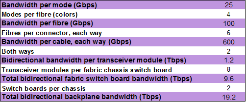
Each of the two backplane fabric chassis switch boards contains two fabric switch ASICs to handle traffic between the ten sleds and the optical rack backplane. Each 18-port chassis switch connects to all ten sleds and to the eight optical transceiver modules on its board.
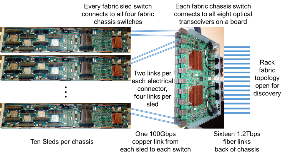
Connecting all the resources in the system with each other via high-speed switches makes The Machine a uniquely flexible R&D testbed. Any workload processor node can address any portion of global memory through a minimum of one fabric sled switch plus one fabric memory interface and a maximum of one fabric sled switch, two fabric chassis switches, and one fabric memory interface.
We will note that 19.2 Tb/sec is over half of the theoretical bandwidth that 80 sleds might generate at peak. While 400 Mb/sec aggregate bandwidth is overkill for a compute sled today, the global memory could potentially soak up most of that bandwidth. HPE did not talk about latencies in its switched network, which is reasonable given that many of the key switching components are FPGAs and first generation ASICs, so we look forward to checking back with HPE in a couple of quarters.
Server Chassis With . . . Lasers
HPE uses vertical-cavity surface-emitting laser (VCSEL) technology in this first R&D testbed design. VCSEL technology is more mature than silicon photonics (SiPh), but it means that HPE had to build multi-chip modules to package VCSEL arrays with the high-speed logic needed to interface to the fabric switch. The innovation that makes this possible is an inexpensive diffraction grating that makes it easy to both align VCSEL transmitters and receivers with the individual fibers in a cable and to additionally multiplex four colors of laser light into each fiber.
Optical switching rates for both VCSELs and SiPh emitters and detectors have been economically stuck at 25 Gb/sec for a few years. Cost-effective optical solutions can increase bandwidth by either adding more 25 Gb/sec single-mode fibers to a cable and connectors, which adds considerable cost, or by multiplexing multiple 25 Gb/sec modes onto fewer fibers. The diffraction gratings required to do this have been expensive, but HPE’s X1 low cost plastic diffraction grating changes the economics of the solution.
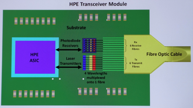
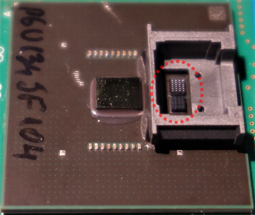
The multi-chip transceiver module makes it easier to combine high-speed logic with VCSEL technology. While the rugged, but inexpensive, new fiber optic connector makes it much easier to connect the transceiver modules to standard fiber optic connectors in the back of The Machine’s chassis. The figures below show how HPE’s fiber optic connector fits onto the HPE X1 optical transceiver module.
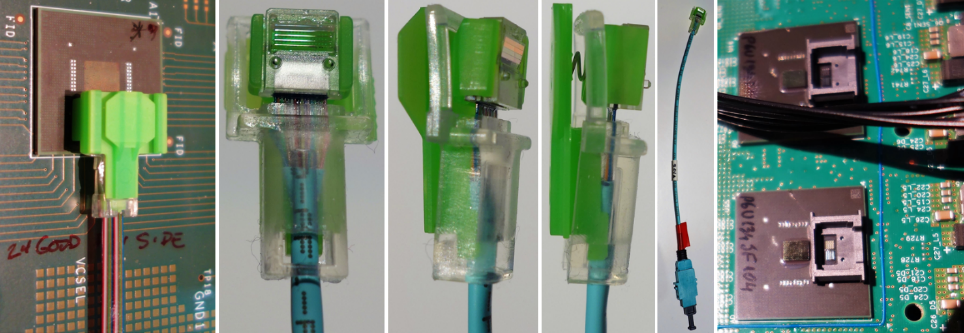
From left: optical transceiver module test harness with cable connected, views of cable connector diffraction grating and mechanical assembly, entire cable including back of chassis connector, and rack backplane switch motherboard with optical transceiver modules mounted.
While the VCSEL based transceiver module is inexpensive enough for HPE to build The Machine R&D testbed and potentially integrate with shipping products, HPE’s goal is a home-grown multimode SiPh solution. The primary difference between VCSEL and SiPh are:
- VCSEL’s emit light straight up, out of the plane of the die, requiring connectors, and means of bending light on top of a VCSEL chip. SiPh emits light in the plane of the silicon, out to the side of the die, so light pipes can be routed on top of or inside of a motherboard.
- VCSEL’s switch their light on and off, while SiPh acts as a shutter for a constant light source. This is one of the reasons that low-cost multimode SiPh technology is so difficult to develop.
- VCSEL’s require a different manufacturing process than logic, so coupling VCSEL’s with logic requires multichip packaging, and other chips cannot be packaged on top of the VCSEL die. VCSEL die must also be exposed to air on top of the package. SiPh can be layered with logic die anywhere in a vertical stack, and potentially layered with logic on a single die. SiPh emitters and detectors are located on the side of a package, and light pipes can be integrated into the package so the SiPh die is not exposed to air.
- VCSEL’s are a mature technology today, while SiPh is an immature technology still searching for the right mix of bandwidth, cost, and manufacturability.
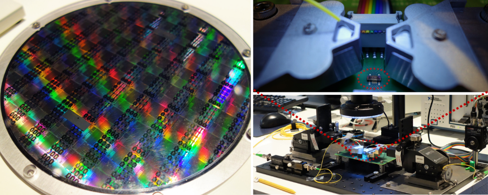
HPE is developing a multimode SiPh technology base which it hopes can replace VCSEL technology over the next few years. The figures below show a couple of marketing aids to demonstrate the theory of the design, a wafer full of the prototype die, and a prototype chip embedded in a test rig.

From left: models of HPE’s SiPh silicon structures to emit specific light frequencies and silicon logic layered on top of SiPh structures, plus a screen shot of the test silicon showing the circular light emitting structures.
Pushing four modes down a fiber cost effectively is challenging, and HPE is justified in being proud of its accomplishment for VCSEL based multimode transceivers. If HPE can duplicate this feat with SiPh, that will be a much bigger accomplishment.
Is It Safe?
Security is one of the major new use cases HPE designed The Machine to explore. HPE has given its security experts a design role in The Machine. Security and fabric boot first, before any other components of The Machine. Data is encrypted at rest (in memory and storage) and each node is protected by a hardware firewall. The firewall design is based on HPE Labs’ experience with multiple generations of Superdome platforms.
Workload processor nodes are only booted when required, and can be powered down completely when not needed. This is important from both a power consumption point of view and a “ghost images” scheduling and malware prevention point of view – when a workload processor is powered down, it can’t run malicious code.
The Machine’s security strategy also has its roots in a “data first” design mentality. The Machine is a testbed for HPE to explore next generation security architectures as well as network, memory, storage, and compute architectures.
Minimizing data movement means that security and permissions must move with both data and applications. For many workloads, data will be persistent while applications that process the data will instantiate close to the data they need to process.
HPE uses node management processors on the global memory plus compute sleds and on the chassis switch boards to boot The Machine’s network. Think of the node management processor as a baseband management controller (BMC) on steroids. Each node management processor contains its own root of trust, and as The Machine’s network boots, the node management processors secure each node in the network. Note that a sled does not need to have a workload processor node to enumerate and boot the fabric memory interfaces – it is a true data-centric architecture.
When a workload processor node is booted, the node management processor on its sled at first constructs a firewall with no permissions. The workload processor node boots via firmware, and as it boots, it enumerates global memory address ranges only as it is allowed through the firewall. As applications run on the workload processor node and require access to more fabric memory resources, the node management processor changes firewall settings. New memory ranges appear to the workload processor and its local OS as hot-add memory. Applications running on the workload processor node only know that they can access the memory they requested. Requests will be denied if the applications have insufficient permissions from the node management processor to access that memory.
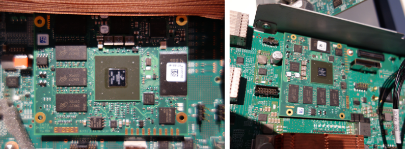
HPE’s The Machine security strategy leverages ARM TrustZone for this initial R&D testbed. We noticed a PHYTEC phyFLEX-i.MX6 module next to both the fabric sled switch and the fabric chassis switch. (See below for photos of this module.) This is the node management processor. The node management processor is always on, so it must be both low power and highly reliable.
The node management processor is based on an NXP i.MX6 embedded SoC, with a quad ARM Cortex-A9 processor operating at up to 1 GHz, with VFPv3 floating point and ARM NEON, 1 MB of L2 cache, and integrated 1 Gbps Ethernet. The node management processor has all the connectivity required to communicate directly with a sideband Ethernet management backplane and to boot a sled’s workload processor and fabric memory interfaces.
The NXP i.MX6 processor implements ARM’s TrustZone security architecture, along with high assurance boot, cryptographic cypher engines, a random number generator, and tamper detection. These features accelerate the node management processor’s role in key management and in provisioning and deprovisioning workload processor nodes.
HPE is a big proponent of and contributor to the Distributed Management Task Force’s (DMTF) Redfish application programming interface (API). Redfish is a RESTful API for “simple and secure management of modern scalable platform hardware,” that is, scale-out cloud hardware. HPE has redesigned its OneView converged management and integrated automation platform as a layer on top of Redfish. HPE is adapting Redfish for The Machine, which will enable preferred customers and partners who want to experiment with The Machine to use their own cloud management frameworks or HPE OneView.
Software Development
The Machine is intended to support current processor-centric software development methodologies as a baseline for experimentation. It is also a research vehicle for developing new memory-centric software development methodologies and underlying runtime infrastructure. As with any new hardware architecture, there are three general means of migrating software workloads:
- Adapt existing APIs to underlying structure. This is usually straightforward, but also usually provides only nominal acceleration to target workloads. In the software world, this equates to a minor code revision. Validation is simply a matter of making sure that the revised application runs on the new hardware.
- Recode existing algorithms. This requires in-depth knowledge of the new architecture to optimize the performance of critical sections of an application. In the software world, this is a major revision, requiring that the results of the new code be validated for correctness. The extra optimization work results in dramatically better performance than simply adapting the APIs to run on the new hardware. This technique will not capture all a new architecture’s theoretical performance.
- Design entirely new algorithms. This is where software developers must think differently about their application and completely refactor their requirements against the new hardware. It is not optimization, it is redesign.
Existing applications can run on The Machine without modification, but modifying application architecture should net developers substantial returns on their coding investment.
One of the big payoffs for software developers is eliminating the additional global memory access latencies of the two fabric chassis switches and the optical connection between them. That requires moving an application to a workload processor node that is located on the same sled as the current subset of data being processed. A workload might be migrated across many sleds as it processes different portions of a large data set to maintain sled locality. The coding semantics required to enable average developers to do this have not yet been developed. That is one of the goals of The Machine.
Software research is dependent on hardware research. Some theoretical work can be done using simulations, but not the market enabling work that needs to happen over the next five years as pervasive non-volatile memory becomes a reality. The Machine is the hardware base that will enable software researchers to experiment with complete new architectural concepts in real-time, instead of with painfully slow partial system simulations.
Conclusion
HPE’s goal for The Machine is to work through hardware and software co-development challenges to enable large, scale-out, non-volatile memory systems.
Moving network switches into server architecture is not a new concept (see U.S. patent 6,035,366, granted in 2000), but previous work has not substantially impacted commodity data center hardware. HPE has taken switch based architecture into new territory with The Machine’s “memory-driven computing” R&D testbed. HPE built a testbed that can host new memory and processor products without much additional design work, and the company did that by building a brand new in-rack switch based network architecture from scratch.
HPE mentioned that The Machine uses several design concepts from its Superdome high-performance systems, for example, the switch-based architecture and load balancing across the switch planes. We don’t think HPE intends to commoditize Superdome architecture though The Machine. To our thinking, HPE’s direction is taking mainstream compute architecture to the next level by borrowing some of the advanced architectural concepts used in Superdome and The Machine.
HPE acquired SGI in August 2016, and SGI appeared across the aisle from HPE at the SC16 expo floor in November. SGI also brought some of its demo gear to HPE Discover London in early December. The Machine is complimentary to HPE’s recent acquisition of SGI. SGI brings new advanced memory coherence experience and architectures into HPE, which should help improve The Machine performance over time. As HPE explores new design points with The Machine, we would look to some of the first fruits of that exploration to appear as SGI-branded, large memory, switch-based, rack scale systems. And as the two companies integrate, we anticipate we will see variants of The Machine with much more capable workload processor nodes.
HPE’s The Machine is exactly the kind of architectural R&D investment and testbed we expect to see from a first-rate computer architecture lab.
Paul Teich is an incorrigible technologist and a Principal Analyst at TIRIAS Research, covering clouds, data analysis, the Internet of Things and at-scale user experience. He is also a contributor toForbes/Tech. Paul was previously CTO and Senior Analyst for Moor Insights & Strategy. For three decades Teich immersed himself in IT design, development and marketing, including two decades at AMD in product marketing and management roles, finishing as a Marketing Fellow. Paul holds 12 US patents and earned a BSCS from Texas A&M and an MS in Technology Commercialization from the University of Texas’ McCombs School.




Be the first to comment