

Not all of the new and interesting high performance computing systems are always in the upper echelons of the Top 500 supercomputing list, which was announced at the opening of the SC16 supercomputing conference in Salt Lake City this week. Sometimes, an intriguing system breaks into the list outside of the top ten or twenty most powerful machines in the bi-annual rankings of number-crunching performance, and such is the case with the new “Saturn V” supercomputer built by Nvidia using its latest GPUs and interconnects.
The Saturn V system, nick-named of course for the NASA launch vehicle that eventually took men to the moon for the first time in 1969, is actually installed at Nvidia itself and it looks a bit like the kind of machine learning systems that it hopes enterprises will install and use not only to run AI workloads, but also to do other kinds of work, such as traditional HPC simulation and modeling as well as database and analytics acceleration.
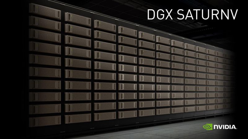
The Saturn V cluster is comprised of 124 of Nvidia’s own DGX-1 hybrid CPU-GPU systems, which were launched last April by the company and which were explicitly created to foster the use of its high-end “Pascal” Tesla P100 GPU accelerators, which also debuted at that time. The Tesla P100s come in two flavors, the original that mounts directly on the motherboard and that links to the processing complex over NVLink interconnects, called the SXM2 form factor, and the other having roughly the same performance and HBM2 stacked memory capabilities – and unfortunately the same name – but hooking to the CPU complex in a system over normal PCI-Express 3.0 x16 links.
The Tesla P100 SXM2 card has 3,584 CUDA cores on its massive GP100 chip, which run at 1.33 GHz and which can burst to 1.48 GHz, delivering a maximum of 5.6 teraflops of floating point performance at double precision (64-bit), 10.6 teraflops at single precision (32-bit), and 21.2 teraflops at half precision (16-bit). These cards weigh in at 300 watts, but deliver 17.7 gigaflops per watt at double precision, which is almost twice that of the prior generation of Tesla K80 accelerators, which have a pair of “Kepler” GK210B GPUs on a single card and that have considerably less memory bandwidth and a little less memory than the Tesla P100 devices.
The Tesla P100 cards probably have a list price on the order of $10,500, too, we estimated back in April, based on the $129,000 price tag of the DGX-1 system, which has eight of these accelerators. If you back out the cost of the underlying Xeon E5 server that is hosting the Tesla P100 cards in the DGX-1 machine and then take out the value of the AI software stack and support charges for it that Nvidia is charging, you can sort of reckon the cost of the GPU compute portion of the system. The Tesla K80s probably cost on the order of $4,000 on the street today, with the PCI-Express versions of the Tesla P100 cards hovering around $5,000. Basically, NVLink support and the SXM2 form factor doubles the cost of the GPU compute element. (We compare the last three generations of Nvidia Tesla GPUs here, including the new Pascal P4 and P40 accelerators, which do not support HBM2 memory but rather slower GDDR5 memory but which have the best performance per watt on single precision work that Nvidia offers.) The PCI versions of the GP100 cards actually deliver slightly better gigaflops per watt because they only take a slight performance hit dropping their core clock speed down to 1.13 GHz but the power consumption drops down to 250 watts.
Suffice it to say that Nvidia has lots of options when it comes to GPU acceleration, and customers have to plan very carefully about which one they install. Those who have mixed workloads will need to pay a premium for the broader cards, of course. (This is so by design, and it is the nature of the modern chip business.)
The original DGX-1 launched in April has two 16-core “Haswell” Xeon E5-2698 v3 processors, which run at 2.3 GHz and which are rated at 3 teraflops running in FP32 mode according to Nvidia. The CPU side of the system is equipped with 512 GB of DDR4 memory, which is a reasonable amount. The eight Tesla P100 accelerators each have 16 GB of HBM2 stacked memory on their package and are implemented on the mezzanine planar and linked in a hybrid cube mesh network to each other. Using half-precision FP16 data storage in the GPU memory, the eight Pascal GPUs can deliver 170 teraflops of aggregate performance for deep learning algorithms. Cut that to 42.5 teraflops total for double precision math. The planar on the DGX-1 system has a PCI-Express switch on it to link the GPUs to a pair of two-port 100 Gb/sec InfiniBand adapters from Mellanox Technologies and a pair of 10 Gb/sec Ethernet ports that come off the Xeon chips. The system has four 1.92 TB flash SSDs for high bandwidth storage, which is necessary to keep the CPUs and GPUs fed. The DGX-1 fits in a 3U enclosure and burns 3,200 watts across all of its components.
We expected for the DGX-1 to be very powerful as a server node with strong scaling, as the HPC people say, but with the current Top 500 list, we get to see how the DGX-1 performs in a clustered environment. To create the Saturn V cluster, Nvidia got some 100 Gb/sec EDR InfiniBand switches from Mellanox and hooked 124 machines together in a fat tree network. (We think that if Nvidia could make more of the P100 SXM2 modules and keep more of them for itself rather than distributing them through the channel with partners such as IBM, with its Power Systems LC “Minsky” system, and Quanta Computer, with its QuantaPlex system, it might have built an even larger Saturn V. And as the Tesla P100 SXM2 modules ramp in production, we expect that it might radically extend the internal cluster.
Ian Buck, vice president of accelerated computing at Nvidia, did not divulge any future plans that the chip maker might have on the tenth anniversary of the launching of the CUDA GPU offloading paradigm that he helped create. But he did tell The Next Platform that on an initial run using 36 DGX-1 nodes, the system could deliver peak performance of 1 petaflops on the High Performance Linpack (HPL) parallel Fortran benchmark test that is used to gauge the relative performance of machine on the Top 500 list. That worked out to 10 gigaflops per watt. On the full 124 node Saturn 5 system, which had the CPU side of the complex upgraded to 20-core “Broadwell” Xeon E5-2698 v4 processors that run at 2.2 GHz, the machine had a peak performance of 4.9 petaflops and delivered 3.31 petaflops of sustained performance. That means 67.5 percent of the flops available in the system ended up being used for actual Linpack work. This is not a great efficiency, but it is not out of the ordinary for a new architecture that still needs some tuning and it no doubt could be a lot better if Intel supported NVLink ports on its Xeon processors. (Some of the four NVLink ports would be consumed by the CPU connections, and that would mean the DGX-1 would have fewer cross-linked GPUs sharing a virtual memory space. And that would impact performance, too.)
Nvidia did not provide a price for the Saturn V cluster, but we reckon that if you add in the EDR InfiniBand networks for the dozen and a half racks it takes to hold the Saturn V system and take out the value of the AI software stack that is not useful for running Linpack, and use internal storage on the nodes instead of an external parallel file system like Lustre or Spectrum Scale (GPFS), then this machine would cost somewhere on the order of $14.7 million after discounts, or about $3,000 per teraflops peak. The Saturn V machine consumed only 350 kilowatts in total, yielding a 9.46 gigaflops per watt rating, which will make it the most power efficient system in the world as ranked on the Green 500 list, more than seven times as energy efficient as other systems on the list, according to Buck.
The Saturn V cluster, which is ranked number 28 on the Top 500 list, is not a publicity stunt, either, in case you are wondering.
“This system is internally at Nvidia for our self-driving car initiatives,” says Buck. “We are also using it for chip and wafer defect analysis and for our own sales and marketing analytics. We are also taking the framework we are using on this system and using it as the starting point for the CANDLE framework for cancer research. You only need 36 of these nodes to reach one petaflops, and it really speaks to our strategy of building strong nodes. The small number of nodes makes it really tractable for us to build a system like Saturn V.”
Here is the cool thing. Nvidia is not using the Saturn V cluster to run EDA software used in chip design, but rather is using neural networks to analyze chip and wafer defects. So it is not AI next to HPC so much as AI aimed at HPC.
Some other things to contemplate. Here’s the fun bit to contemplate. Nvidia has demonstrated it can deliver 42.5 teraflops of peak performance and about 28.7 teraflops of sustained performance in a 4U server node. That is about 10.6 teraflops per 1U of rack form factor space. IBM, Nvidia, and Mellanox are working to get more than 40 teraflops of capacity into a 2U “Witherspoon” system next year with the “Summit” supercomputing they are building for the US Department of Energy facility at Oak Ridge National Laboratory. To our way of thinking, that means the future “Volta” GV100 accelerator cards should have about twice the performance of the Pascal GP100 cards currently shipping, if IBM sticks with the 2U form factor and only puts four GPU accelerators into the Witherspoon box alongside a pair of 24-core Power9 chips as we expect. And by this time next year, Nvidia might be able to build a DGX-2 system sporting Intel “Skylake” Xeon E5 v5 processors paired with eight Voltas and delivering as much as 85 teraflops double precision in a 3U chassis – better performance density than the Summit machines at the peak level. We still think the Witherspoon node used in the Summit machine could have a slight advantage in harnessing that floating point oomph across four Volta cards for HPC workloads. So it might be a wash.
If AMD supports NVLink ports on the future “Zen” 16-core Opteron processors, this would be a very interesting development indeed. But that seems unlikely, considering how AMD has joined the CCIX, OpenCAPI, and Gen Z consortiums. That said, it could happen, and that would mean customers wanting to tightly couple CPUs and GPUs in a fat node could have an X86 option that had many of the same benefits that IBM is bringing with Power8 and Power9 chips.


GPU Engines Are So Strategic China Will Have To Use Its Own
China is the world’s second largest economy, it has the world’s largest population, and it is only a matter of time before has a world-class technology ecosystem spanning the smallest transistors to the largest hyperscale and HPC systems. It simply has enough money, and enough time, and enough smart people, …
“Hopper” GH100 GPUs Are The Heart Of A More Expansive Nvidia System
There are a lot of things that compute engine makers have to do if they want to compete in the datacenter, but perhaps the most important thing is to be consistent. The devices they make have to consistently push the technological envelope, and that have to be delivered in volume …
Taiwan’s Fastest AI Supercomputer Goes To Foxconn
Back in the day, when the AI revolution was young, Nvidia co-founder and chief executive officer used to make the rounds with each new generation of datacenter GPUs and provide the first DGX systems based on any particular GPU to marquee customers. Sam Altman and Elon Musk, co-founders of OpenAI, …
“Nvidia did not provide a price for the Saturn V cluster, but we reckon … this machine would cost somewhere on the order of $1.3 million”
124 nodes * $129k unit cost for the DGX-1 = $16 million, and that’s without any switches, cabling, racks etc.
You can buy systems with 4 SXM2 Tesla P100s for less than 50K already.
IBM will problably put 6 gpus and 2 power9 per node. Also much better main memory bandwidth w.r.t. intel or AMD. Better for nvidia to stick with Ibm power rather than helping Intel in how to build the PHIs. FPGAs are the next