

Being too dependent on one source for a key component is not just a bad idea because of supply chain risks, but because it can result in higher prices.
Intel customers don’t need to be reminded of the lack of direct competitive pressure in the X86 chip market for servers, because they remember what competition that felt like. And customers and system makers that had taken a risk with AMD Opteron processors a decade ago don’t need to be reminded of either of these facts, particularly after AMD walked away from the server business in the wake of technical problems with the Opterons during the Great Recession, which unfortunately for AMD – but certainly not for Intel – coincided with the rise of the Opteron-like “Nehalem” architecture of the workhorse Xeon platform.
The situation a little less than a decade ago could not have worked out better for Intel and worse for AMD. But turnabout is fair play, and with the “Zen” cores that AMD unveiled at Hot Chips this week in Silicon Valley, which will appear in various server products next year, AMD is getting back in servers and looks like it wants to stay there for the long haul.
It will be a long haul, of this we are sure. But the first step is to get a decent architecture into the field, one that can stand toe-to-toe with the Xeons and win some deals.
This is no easy task, as every server processor maker – those that are left – will tell you. Intel has lived by the adage that only the paranoid survive, and to its great credit, the chip giant has behaved like it has been under intense competitive pressure in the past decade in order to keep pushing innovation in the server space and as it expands out further into storage and networking. This is not an easy thing to do when you have 97 percent market share. But there is no competition like real competition, and no matter what, to mitigate risk and to bring competitive pressure to bear, all of Intel’s largest customers, whether they are hyperscalers and cloud builders or the server OEMs and ODMs that make iron for them, want an alternative. And an X86 alternative is easier for them to consume than an ARM or Power option. It also presents the juiciest target in the datacenter by far in that Intel has around 50 percent gross margins in the server chip business – which it has sustained, more or less, since AMD left the field – that is growing at 10 percent to 20 percent per year. Hitting that target is not easy, particularly as Intel has either created or acquired the technologies to keep a diverse portfolio of compute pushing back against all the CPU, GPU, DSP, and FPGA alternatives.
To get customers back for its X86-compatible Opterons, AMD is going to have to win back the trust of server makers and their customers, and this will take time, perhaps longer than it did the first time around with the “Hammer” family of Opterons. Or, if the price pressure is high, maybe not. Maybe there is a built in 10 percent share just waiting for AMD to capture it.
Back at the dawn of the Opterons, the market was spoiling for a fight back then, too. A decade ago, at the height of the Opteron revolution in the datacenter, AMD was riding high. The Hammer family of chips more than a 64-bit X86 alternative to the 32-bit Xeon. The Hammer architecture was designed with innovative technologies like HyperTransport, which Intel did not have anything like until the QuickPath Interconnect debuted in 2009 with the “Nehalem” Xeons. Intel made a bad choice in the early 2000s, and wanted customers to move to Itanium to get 64 bit processing and addressing, and it wanted to charge a premium for that. AMD brilliantly shot the gap between the 32-bit Xeon and the 64-bit Itanium, and eventually had 25 percent share in segments of the server market. But the technical issues with the “Barcelona” Opterons coupled with the economic ones caused by the Great Recession and the very good Nehalem chip design from Intel were too much for AMD to take. Thor went from scuffling with a surprised Bruce Banner to facing the Hulk, who as we all know is always angry.
So you can understand, after that experience, why AMD is a bit Zen – quite literally – about how to get back into the server space and stay there.
Zen And The Art Of Server Business Maintenance
“I think of Zen as balance,” Mike Clark, the senior fellow and lead architect at AMD who steered the design of the Zen core, explained in rolling out its design. “And I think of my job as an architect as trying to balance all of the competing forces. You are given a transistor allocation, and you want to use the transistors as best you can and build the best core you can. But there are the competing interests of clock frequency, how much work you can get done per clock, the power, the complexity of the ISA, which you have to get functionally correct and new instructions you might want to add. We were working on the Bulldozer line, and we were improving with the Excavator core, learning, but we could see that we needed to make some bigger changes. If you try to make a big change in the architecture, however, it really throws off the balance. You realize you need to rebalance everything and do a grounds-up core. We set a goal of getting 40 percent more instructions per clock while keeping the other forces at bay, and set a new point for the architecture that we could build on going forward.”
Because AMD is resource constrained – and we would argue because prior management ceded the server market too easily to Intel – it made a choice to collapse its desktop and laptop cores into its server cores and also try to come up with a core that could span from fanless laptops to supercomputers. This is not an easy task, and it remains to be seen how successful this Zen core will be down at the low end. But the early indications are that the Zen core and the chips that will be derived from it are brawny enough to be good for servers, and here at The Next Platform, that is what we care about anyway.
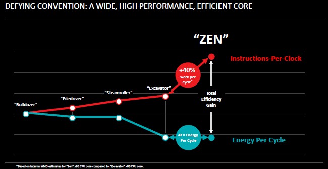
Getting 40 percent more work through a core while keeping the power consumption flat, as AMD has done with Zen, is no mean feat. The company had to not only radically change the core design, but also change the process by which it balances performance and power as it is designing a chip. Cranking up the performance usually means blowing off more heat, and then you have to slow the chip down to get into thermal envelopes that people can live with, which sacrifices performance.
“Architects are pretty crazy, but we knew we had to take a different approach,” said Clark. “We have been working on the frequency and the performance for decades, and we have really good tools for this. We have really good tools for power as well. But we had never really intersected power at the beginning of a grounds up core into the microarchitecture, really looking at every feature we are adding and being able to really understand the power it was going to draw running real workloads and evaluate a feature trade off that early in the design process. We were usually applying the power analysis much later in the design flow, really at a point where the key architectural decisions had been made and there was way less flexibility to go attack any power problems. They might be fundamental in the architecture.”

The Zen microarchitecture is very different from that used in the Dozer family of server cores that followed the Hammer cores to market and, quite frankly, did not do as good of a job competing against Intel as they needed to.
The Zen core is a much wider and deeper machine than the Dozer cores it replaces, according to Clark, and it has a radically altered caching hierarchy that can keep it fed with data and instructions.
Clark said that the Zen core has much better branch prediction, and that one of the biggest new features was a large op cache. “In the X86 architecture, there is a variable instruction length and this makes trying to find multiple instructions to get going in the machine a very difficult problem because it is a serial process. To attack that, you build a pretty deep pipeline and you spend a lot of logic, it burns a lot of power. Having seen instructions once come through the pipeline, we now have the micro-ops and we can store them in an op cache and store them so that the next time we hit those instructions, we can just pull them out of the op cache. We can cut stages out of our pipeline when we are hitting the op cache and we can use those high power decoders and not burn all that power as well removing the state we can also deliver more ops into the machine per cycle, too. This is a really great feature that delivers us way more performance and saves us power at the same time.”
The Zen core has four integer units (ALUs) and two address generation units (AGUs) plus two load/store units and two floating point units. The core can dispatch six micro-ops per clock instead of four with the Excavator core that might have in theory been used in the Opteron 6500 processors had they ever launched. (Which they didn’t. The “Warsaw” Opteron 6300s were the last of the Opterons, and they came out in June 2013.)

Another big change was to shift to a write-back L1 cache for the core, rather than the write-through L1 cache used in the Excavator, which was less power efficient. The L2 and L3 caches are similarly faster as well as larger, and that means that the fetchers that are looking to match instructions with data have a better chance of finding the data in the closest cache to the execution units. The bandwidth on the L1 and L2 caches is double that of the L1 and L2 caches on the Excavator cores, and L3 bandwidth was increased by more than 5X. For the cache hierarchy, the Zen core has 64 KB of L1 instruction cache and 32 KB of L1 data cache. Each core also has a 512 KB L2 cache that can store either instructions or data, and each core has a port into a 2 MB segment of a unified 8 MB L3 cache. All the caches are linked by 32 byte ports to the L3 cache and all cores can see all elements of the L3 cache with the same latency.
Clark only talked about the Zen core, not the stuff that wraps around it. So we have no sense of the main memory configuration, integrated PCI-Express and Ethernet controllers, or any other goodies that should be on or near the die. But we are digging around.
The integer and floating point units in the Zen core have a coprocessor model, as Clark put it, with separate schedulers and register files for each. The floating point unit has a two-level scheduling queue, with two pipes each with one multiplier and one adder. The floating point unit supports two 128-bit vectors, which means it can do four double precision operations per clock or eight single precision operations per clock; as far as we know, FP16 half precision floating point is not supported on the Zen core. Intel is able to do twice as many floating point operations per clock with the current “Broadwell” cores used in the Xeon line, and four times as many with the “Knights Landing” Xeon Phi cores. The Zen floater has two units for accelerating AES encryption and supports SSE, AVX1 and AVX2 floating point operations as well as SHA hashing and is compliant with legacy MMX and X87 instructions, too.
Here is what the Zen CPU complex looks like when you add it all up:
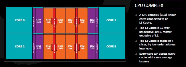
AMD is using this four-core segment as the basic building block for its processors, and obviously it could be cut down to be as small as one or two cores and even doubled up to eight or sixteen cores if need be, either through a single die for the larger chips or through multichip modules. Yields are better on smaller chips, and AMD is expected to use multi-chip modules for its largest Zen Opteron processors. (We will get into that in the follow-on Zen story.)
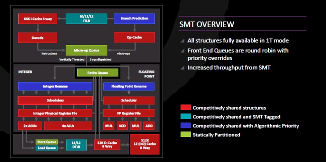
In addition to all that, the Zen cores support AMD’s first implementation of simultaneous multithreading (SMT), which you will never catch an AMDer call HyperThreading. That is the name that Intel uses for its brand of SMT in the Atom, Xeon, and Xeon Phi processors. In both cases virtualizes the pipeline in the cores to make it look like two virtual pipelines to the operating system, allowing for more work to be pushed through the chip in many cases. For the strongest and most predictable single-threaded performance, users turn SMT off. Some chips, like IBM’s Power family and Oracle’s T, S, and M series Sparcs, the chip can dynamically scale the thread levels as workloads dictate or require.
With prior Opterons using the Dozer line of cores, the AMD core design did not always yield the best single threaded performance. With the Zen core, Clark said that the idea was to make sure that all of the key resources would be available for a single thread when this was critical for performance. We presume that customers will be able to turn SMT on and off at will through hardware settings and to have it set automagically by flags in the operating system to dynamically turn it on and off as particular applications run on a server. (This dynamic SMT setting is important when you can have 2, 4, 6, or 8 virtual threads per core and programmers are not always able to reckon what the best setting might be.) The other side of the SMT is that when there are two threads running, you want as many resources on the core to be competitively shared so the two virtual threads can interleave work across the elements and boost the overall throughput of data and instructions through the core.
AMD did not provide any insight into how much performance boost it will see from SMT, but obviously it will depend on workload and its sensitivity to threads, as is the case with all SMT. We asked if AMD was interested in pushing the SMT beyond two virtual threads, and Clark said with a laugh that he was focusing on two threads for now.
Here is the nitty gritty detail on how the Zen core has been tweaked compared to the Excavator core:
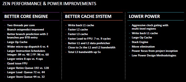
Add that all up, and you can see how to get to 40 percent more instructions per clock, and hopefully, the clocks on the Zen-based Opteron processors are high enough that machines with 4, 8, 16, and 32 cores will be able to have high throughput as well as high single-threaded performance. (We will be doing a follow up story on the expected Zen Opteron server chips and how they may pan out.) But AMD also has to keep the power consumption down. In addition to the micro-ops cache and the write-back L1 cache, the Zen cores have aggressive clock gating with multi-level regions throughout the core. There are a bunch of other tweaks to boost performance, reduce power, or both.
The Zen chips are etched using 14 nanometer FinFET processes from Globalfoundries, the company that has the former AMD chip fabs as a key part of its business. The desktop version of the Zen Opterons, code-named “Summit Ridge” and having eight cores, will come to market in the first quarter of 2017, and the first server variant, called “Naples” and having 32 cores, will follow in the second quarter.
“We like to say that AMD is back in high performance X86 compute, but we are not just back – we are here to stay,” Clark said emphatically after concluding his presentation. “Zen was not a destination, but just a stop on the way to more performance. We are committed to continue to push high performance X86 compute going forward in the roadmap.”
So yes, there is a Zen+ chip, and it is already in the works. The game is afoot, and next up will be AMD’s K12 ARM.

Fat Server Spending Props Up Slowing AI Servers At Dell
Just because you are the number one supplier of servers, storage, and PCs in the world does not mean the job of building those machines and making money is easy. It is not, and the financials of Dell Technologies shows just how tough it can be even when things are …
“El Capitan” Supercomputer Blazes The Trail for Converged CPU-GPU Compute
Every couple of years, Lawrence Livermore National Laboratory gets to install the world’s fastest supercomputer. And thankfully the HPC center usually chooses a machine that not only fulfills its mission of managing the nuclear weapons stockpile of the United States military, but also picks a mix of technologies that advances …
What Faster And Smarter HBM Memory Means For Systems
If the HPC and AI markets need anything right now, it is not more compute but rather more memory capacity at a very high bandwidth. We have plenty of compute in current GPU and FPGA accelerators, but they are memory constrained. Even at the high levels of bandwidth that have …
Only 128bit floating point units 🙁 sounds already a bit outdated
Just sounds. Half of the world still doesn’t know what to do with mmx (see javascript). I’d say 128bit is plenty for the forseeable future for general purpose cpu. What I would like to see instead are 4 memory channels (instead of usual 2) to feed those FPUs. That would make much more difference for engineering workloads and would be good fit for budget workstations (intel knl with six mem channels and hbm is currently the best you can get in workstation size).
If you are IBM/Oracle and you actually have the extra SMT hardware/execution ports to support the extra processor threads above 2 then Yes by all means make something that can be varied, but for the very base level of SMT that requires at least enough hardware to support 2 SMT processor threads it would be more efficient to stay at two threads, as that way if any one of the two threads on the same core stalls the core’s execution resources can be given over quickly to the other processor thread and the other thread’s instructions can be used to fill any pipeline bubbles with useful work while the stalled thread’s latency/Dependency is resolved.
The very Idea of having SMT in the first place is that at the very basic minimal level of SMT(2 Processor Threads minimum) there exists a readily available set of SMT hardware resources to extract as much work as possible from a CPU’s core that at the least supports SMT2(2 processor Threads per core)! And any single threaded processor core not SMT capable has to live with some unused pipeline bubbles for lack of the SMT capabilities in its hardware to properly and efficiently context switch between two processor threads to avoid any execution pipeline under-utilization/wasteful pipeline bubbles and other inefficiencies that occur when a thread has to wait for some other event to occur.
All SMT processors do have the ability to disable their SMT functionality for testing/debugging and other uses, but why have SMT ability in the first place and not use it! It’s not like these Server SKUs are going to be used for any real time sensitive sensing functions in the first place they are there to work as many threads as are available for 2 SMT threads, or above, with SMT2 being the minimum number of threads that must exist to make better use of a CPU core’s execution resources should one thread experience a stall/dependency that requires a stall/wait. AMD’s Zen is supposed to have that ability to prioritize processor threads, and there is always preemption to take into consideration via the OS/Hardware and other functionality for the giving of higher priority on the software/hardware interrupt level.
There really needs to be some more time for some Zen white papers and the compiler optimization manuals to get wider publication, in addition to a little more information from AMD on just what type of coherent interconnect fabric exists beyond the 4 cores in that minimal 4 core complex as well as what exists to deal with more complexes up to the 8 total(4 core complexes) that make up the largest 32 core Zen server SKU.
I have my suspicions that this first consumer desktop variant that we have seen tested is actually half of a 16 core server variant put together while AMD was focusing on getting back into the server market, first and foremost! So AMD just took half of that 16 core design and made the slight modifications to get the first consumer Zen desktop variant to market ASAP. Intel does the same this with its High end Consumer E variants being derived from the server SKUs and slightly modified with some server functionality disabled removed. So AMD took half of a 16 Zen Server design and taped out an 8 core die from that larger modular server core plan and created its first Zen Desktop variant with 8 Zen cores per die.
More information is needed before the final measure of just what AMD will do with its 16 and 32 core Zen server variants. Will there be 16 core monolithic Zen Dies, and well as 32 core monolithic die variants for the server/HPC markets, or will AMD go with 2, 16 core monolithic dies on an MCM module for the 32 core Zen Variant! One thing is certain AMD is very well experienced with fitting thousands of cores and larger core units(ACE Units) on a single monolithic die and creating some very high performing coherent interconnect engineering between the various cores on a GPU, so that Zen 32 core variant this time around could very well be of a monolithic design, the only logical reason to maybe go with smaller dies on a MCM module is most likely the wafer yield advantages that come with using smaller dies to begin with.
The other big question that I have regarding any Zen Variants for low power mobile usage is will AMD again be utilizing its high density design libraries in the design/layout of any mobile only Zen 4, or 2, CPU core with GPU, Zen APU variants, that will be clocked lower for mobile usage in the first place! AMD took its high density design libraries normally used for densely packed GPU layout and used those libraries to layout Carrizo’s Excavator cores at 28nm! And by doing so, AMD was able to save an additional 30% in the total area it took to get the CPU core’s layout done without having to have a process node shrink. So AMD was able to re-layout Carrizo cores at 28nm and get that 30% space savings and use that space of other things like more GPU resources and such, at the expense of not being able to clock Carrizo’s cores as high as a core that was laid out using a low density nominal CPU core design layout libraries.
So if mobile CPUs are going to be clocked lower anyways because of thermal/power constrains regardless of how high the CPUs/APUs cores may be able to go. Will AMD again make use of its high density design libraries to layout a Mobile Zen core/APU variant, and get that 30% space savings on top of the space saved by the process node shrink to 14nm. There appears to be some possibility for AMD to get a very densely packed Zen core with using these high density design libraries and having even more room to really beat Intel on the integrated Graphics front by adding even more Polaris ACE units onto some Zen/Polaris APU SKUs for the laptop/tablet mobile markets.