
The lines between a server, a SmartNIC, and a Data Processing Unit, or DPU, are getting fuzzier, and the good news is that definitions do not matter nearly as much as use cases. And with its so-called “spring” Data Center Group launch – note to Xilinx, spring doesn’t start until March 20 this year – the FPGA maker is rolling out its beefiest Alveo SmartNIC to date and talking about the use cases where it makes sense to deploy them – including AI training at the edge, and video analytics, and algorithmic trading at financial services firms.
In all of these cases, the FPGA, surrounded by other blocks of compute and high speed networking, aims to do some of the processing work on a bump in the wire instead of on the CPU host processors in systems. The idea is not only to free up capacity on the CPU, which is an expensive kind of compute that needs to stay focused on applications, usually written in a high level language like Java but sometimes C/C++ for performance reasons, while at the same helping to drop the latency of applications.
The new Alveo SN1000 – Xilinx is not yet calling them DPUs, but it might at some point – and the Vitis development platform for hybrid FPGA-CPU devices is the foundation of the SmartNIC-DPU strategy at Xilinx. (Like we said, it is not clear where to draw the lines, but that will happen in the years to come.)
It is probably useful to remember that the thing that we colloquially call an “FPGA” has been a hybrid compute-network-memory device for a very long time, and the SmartNIC is just an FPGA created in this style with Moore’s Law benefits applied over time to make what would only a few years ago be considered a very powerful hybrid system. For as long as we can remember, so-called FPGAs have included Arm processors, not much but enough for their intended embedded computing purposes and to also ease the pain of programming these devices. In a sense, the malleable programmable logic of the FPGA was an accelerator to the Arm cores on the device, but you could also argue that the CPUs were a serial processing accelerator for the workflow coded in VHDL and RTL on the FPGA logic blocks. The FPGA could also have a chunk of its gates configured as local memory, and ditto for high speed communications on that FPGA, which could be spun up as well. But high-speed SERDES for networking are also hard-coded on the devices these days, and so are blocks of DRAM and sometimes even HBM stacked DRAM memory. Not to get all recursive and all, but the FPGAs themselves are hybrid devices, and they are further embedded into systems that have compute, networking, and memory at a higher level.
The traditional network interface card as most systems have had for most of the past several decades provided a network controller of some kind – most likely Ethernet, but Token Ring has its time as did others, and InfiniBand is still kicking around theses days for high bandwidth, extreme low latency use cases in storage clusters, HPC, and AI. These were based on custom ASICs that plugged into the PCI or PCI-Express bus, bridging the CPU to the network. Over time, ASICs were designed to pull some networking functions off the CPUs, were generally do a pretty good job handling packets but just do not have anything close to the performance of an ASIC designed just to push packets. Over time, as NICs have gotten smarter, more and more offloads were added to the ASICs, and both Altera (part of Intel for the past five years) and Xilinx (soon to be part of AMD) created programmable SmartNICs precisely do they could take on a broader set of offloads and push a wider set of systems software from the CPU out to the SmartNIC. These days, the programmable SmartNIC, as Kartik Srinivasan, director of marketing for the data center group, at Xilinx, has a mix of custom ASIC, Arm CPU, and FPGA compute elements and supports a broader set of offloads from the CPUs, including I/O and network virtualization.
Here is the Xilinx NIC lineup today:
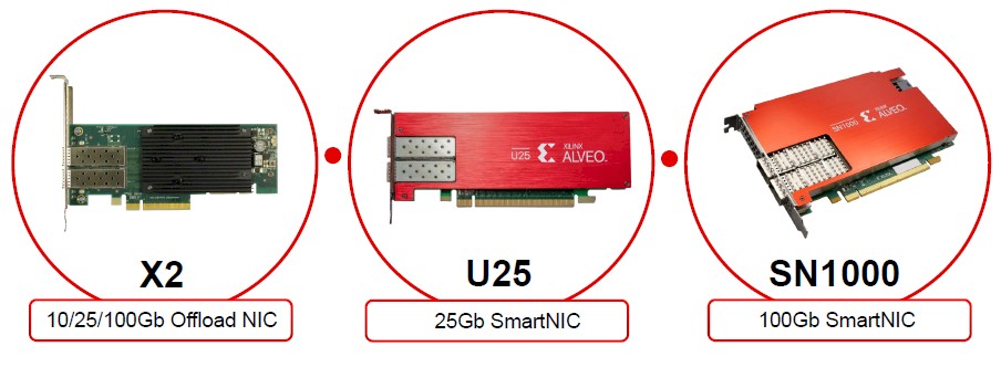
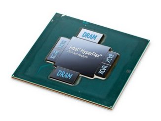
That includes the X2 “dumbNICs” if you want to call them that as well as the Alveo U25 SmartNIC that was announced this time last year, plus the new SN1000 device coming out today. The product line is broader, however, including the Alveo U50, U200, U250, and U280 devices that we took a look at back in August 2019. The Alveo SN1000 is the next generation, and it starts with the SN1022 model that includes an UltraScale+ FPGA with 1 million lookup tables (LUTs) of capacity etched with 16 nanometer processes from Taiwan Semiconductor Manufacturing Corp. The SN1000 also has a 16-core Arm processor cased on Cortex-A72 cores running at 2 GHz, which comes from NXP Semiconductors. That’s a little less FPGA logic capacity than the 1.18 million LUTS in the Alveo U200 card but more than the 872,000 LUTs in the Alveo U50 card. The Alveo U25 card from last year had a Zync-class FPGA and a quad-core Arm Cortex-A53 processor and 6 GB of shared DDR4 DRAM for the device; it had two 25 Gb/sec Ethernet ports, which ain’t much but its enough for a lot of hyperscaler and cloud builder customers for some of their use cases. The SN1000 has 4 GB of DDR4 memory for that Arm CPU and 8 GB of DDR4 memory for the FPGA. The SmartNIC has two 100 GB/sec Ethernet transceivers on it, and comes with a PCI-Express 3.0 x16 or PCI-Express 4.0 x8 interface to server motherboards. The SN1000 is a full height, half length card, and interestingly it requires Red Hat Enterprise Linux or its CentOS clone or Ubuntu Server on the cost machine (meaning the server CPUs, not the embedded Arm CPUs) and supports Ubuntu Server or Yocto Linux on the Arm CPUs inside of the device.
Like other Xilinx SmartNICs, the SN1000 has a variety of onload and offload capabilities. Onload, you say? That’s the Onload/TCPDirect special sauce that Xilinx got from its acquisition of network interface maker Solarflare a few years back, which does a kernel bypass directly into the user space of the Linux operating system (instead of going through the Linux network driver, the TCP/IP stack, and the kernel domain) to accelerate network speeds and drop latency. (These Solarflare cards are in use by 90 percent of the financial exchanges in the world.) The Alveo U25 also has the Solarflare Onload capability built in. There is also the classical offload capabilities for Open Virtual Switch, Intel DPDK, the Virtio-net I/O and virtualization stack for Linux, Ceph object storage client offload, and a slew of hardware-based packet processing acceleration (including VXLAN and NVGRE tunneling encapsulation) that can handle 4 million stateful connections and 100 million packets per second on the FPGA. (Which must be running at around 100 MHz is a 300 MHz Alveo U25 could do 300 million packets per second, as we reported last spring.) If you pushed that packet processing job over to the Arm CPUs, it would be lucky to handle 32 million packets per second, according to Xilinx’s own calculations. The SN1000 has much faster networking interfaces (4X) and still stays within a 75 watt thermal envelope, compared to 50 watts for the U25.
Speaking very generally, the data plane for applications runs on the FPGA fabric, and the control plane for applications runs on the Arm CPUs on the Alveo devices. It used to be that the only way to get to the FPGA fabric was through VHDL or RTL, but now you can use P4 and compile it down to the LUTs. As such, like the Alveo U25, the SN1000 is programmable in P4, C/C++, and high level synthesis (HLS) languages, and all of this is coordinated through the Vitis integrated development environment and runtime. (Vitis, plus access to more revenue streams and more customers, is why AMD is paying $35 billion to acquire Xilinx. The combination of AMD’s ROCm and Xilinx’s Vitis is a counter balance to Nvidia’s CUDA and Intel’s oneAPI.)
You might be wondering why SmartNICs are getting brainer. It’s not just because of Moore’s Law, and Srinivasan explains why.
“Traditional, standard NICs did pretty well through 10 Gb/sec speeds and up to 25 Gb/sec speeds while the CPUs were chugging away at the applications,” says Srinivasan. “The NIC was pumping traffic in and out, and life was good. But 25 Gb/sec started choking the CPU in terms of packet processing, and that gave birth to limited offloads that helped TCP/IP packet processing and often did some high level storage acceleration. Most of them were based on ASICs and did not provide any programmability for either the vendor or the customer. And when datacenters migrated to 25 Gb/sec or 40 Gb/sec, and then 50 Gb/sec and even 100 Gb/sec speeds on the server ports, the CPUs were choking even more. Now, each of the hyperscalers and cloud builders, who have been early adopters of SmartNICs, have their own unique set of requirements and functions that they would like to see offloaded. And they want to have a fast pace of change, evolving every six or twelve months, adding new accelerations and offloads, without sacrificing performance.”
ASIC implementations can’t evolve fast enough, and CPU-only implementations can’t deliver performance, according to Srinivasan. Amazon Web Services would no doubt argue with that, since its Nitro SmartNICs (or DPUs depending on how you define them) are based on a 16-core Arm chip similar to but distinct from its Graviton Arm server chip. But Microsoft, which has deployed the largest fleet of FPGAs in history for its homegrown SmartNICs – probably on the order of several million by now – would concur.
Time to market and cost of solution are two different vectors than any answer has to address, and here is how Xilinx and its financial services customers see the spectrum for algorithmic trading and the possible levels of acceleration:
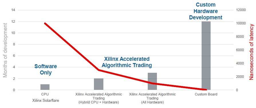
Custom hardware development provides the lowest latency, but it can take a year to get a new ASIC into the field. This is disastrous in an algorithmic trading environment where the game is constantly – sometimes several times a day – changing. Software-only functions running on CPUs have the shortest time to market but the trading applications are on the order of 10 microseconds.
“Our SERDES set a new world record last year, at 22 nanoseconds, tick to trade, with our partner LDA on the UltraScale family,” says Alastair Richardson, global business development manager at Xilinx in charge of the algorithmic trading reference design. That is a “bump in the wire” between the network and the CPU inside of the SmartNIC. “That’s very low when you consider that the latency across a meter of copper wire is 4 nanoseconds and FPGA-accelerated switches from Cisco Systems and Arista Networks can do a port to port hop in 4 nanoseconds.”
Getting data through the PCI-Express bus into the CPU memory takes a long, long time, but taking data from the network and getting it into programmable logic takes on the order of 15 nanoseconds, says Richardson. The reference architecture that Xilinx has put together is a full, complete hardware stack, including preconfigured FPGA “software” for trading, and the example that is ready to go out of the box is a tick to trade application on the Chicago Mercantile Exchange, all programmed in C/C++ using Vitus. Financial services firms that want to play with the big hedge funds and banks can be up and running in weeks, not years.
For video analytics, which just got a little bit harder because we are all wearing masks these days, Xilinx has cooked up an application stack that is accelerated on the FPGAs called Smart World, which aims to deliver deterministic performance with 100 millisecond latency, or about half of an eye blink, figuring out what is in a video stream. This video analytics stack has a range of uses, with a range of performance requirements that looks like this:

This video analytics is an AI inference problem, basically, and all of the data cannot be shipped back to a centralized datacenter to be processed; it has to be done where entities are, right now, and that means edge computing of some sort with acceleration. There are hundreds of billions of dollars in costs – human costs – in these various activities in each sector. The addressable market is about automating some of the monitoring and correlation work that people do, and often do inattentively. Nothing has the patient attention span like a compute equipped with a camera. . . .
As we have pointed out before, Xilinx is up against Nvidia’s T4 GPU accelerators when it comes to accelerated AI inference at a reasonable scale at the edge. (We mean real computing, not a drone or a phone.) Here is how Xilinx thinks the Smart World video analytics stack sporting one each of its Alveo U30 and Alveo U50 cards in an X86 server does against the same server with four Nvidia T4 accelerators; both systems are out in the field and running ResNet-50 and TinyYolo V3. Here is the TCO of the two setups supporting 32 camera streams:
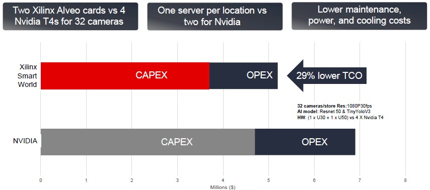
The cost is a bit lower, as you can see, and enough to justify a platform change if you are doing anything at scale. This must be TCO over several years for the money to be so large.
And here is where the FPGA really shines, with latency:
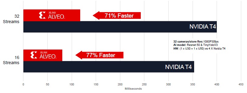
It takes two blinks of an eye to process video images on the servers using the T4 GPU accelerators, and only about a half blink to do it with the FPGA accelerators.
Xilinx and its partners have their eye on adjacent markets in industrial safety, smart cities, smart buildings, and smart retail, and they have tailored hardware to fit the needs:

Xilinx is partnering with Aupera for smart retail and smart cities application, DeepAI for AI training at the edge, and Mipsology to take CUDA code created for systems accelerated with Nvidia GPUs and port it automagically over to FPGA-accelerated systems.


Betting On Extreme Co-Design For Compute Chips
Whether or not the coronavirus pandemic causes the Great Recession II or the Great Depression II, we are without a doubt entering an era when IT industry is going to need lower prices, better performance, and better thermal profiles for their compute engines than they have ever required before. This …
Intel To Set Its FPGA Unit Free To Pursue Its Own Path
Maybe Intel chief executive officer Pat Gelsinger has spent too much time at EMC and VMware. Because now Intel wants to spin out the FPGA business that is a small but bright spot in its datacenter and edge computing businesses. It never made a lot of sense that EMC, the …

AMD Girds For Compute War With Xilinx Deal
The rumors were right, and AMD president and chief executive officer Lisa Su is indeed printing out a tower of stock to acquire FPGA maker Xilinx for what amounts to about $35 billion and, as it turns out, she is relinquishing her position as president to Victor Peng, chief executive …
…”and both Altera (part of Intel for the past five years) and Xilinx (soon to be part of Intel)”…
Whoops! Xilinx is actually being purchased by AMD.
Yeah, just moving too fast for my neurons….
ASIC implementations can evolve fast enough => I think you meant “can’t evolve”
Thanks, correct.