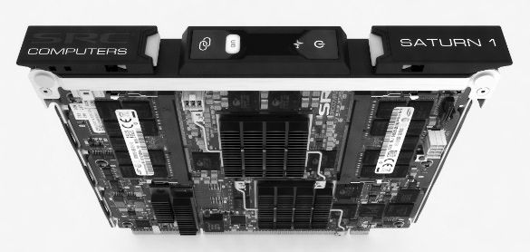
Everybody who is operating at any sort of scale is looking to pack more compute into a smaller space for less money. At The Next Platform, we watch the goings on in the hyperscale and HPC arenas to use them as a polestar for technology adoption among enterprises further down the line. For a lot of different reasons, we think that field programmable gate arrays, or FPGAs, are poised to go mainstream. And a company that was founded by Seymour Cray in 1996, just before he died in a tragic car accident, that has been perfecting hybrid CPU-FPGA systems for military and intelligence agencies agrees and is coming out of stealth to aim its wares at hyperscale datacenters.
SRC Computers, which is based in Colorado Springs, takes its name from Seymour Roger Cray’s initials and was co-founded by the legendary supercomputer designer along with Jim Guzy, one of the co-founders of Intel and until recently chairman of PCI switch chip maker PLX Technology (now part of Avago Technologies), and Jon Huppenthal, who is still SRC’s president and CEO.
SRC shipped its first system to Oak Ridge National Laboratory three years later, and the company pivoted away from the HPC market in 2002 when it started selling its hybrid systems to defense and intelligence customers. Except for a few citations of its machines in academic and lab research, SRC has kept a relatively low profile and its 50 employees – all systems, network, and compiler experts who have been around for a while – have focused on making its MAP hybrid processors and Carte programming environment easier to program and deploy than a typical CPU-FPGA setup. Mark Tellez, director of business development at SRC, says that the company has invested more than $100 million in hybrid systems development since its founding two decades ago.

FPGAs are not a new technology, but they are starting to catch on again in the enterprise and in the HPC sector as processors are starting to hit some Moore’s Law limits. Companies in the financial services and oil and gas industries have tried just about every technology under the sun to goose the performance of their applications and get some competitive edge, and FPGAs have been something they have either toyed with or deployed for specific applications over the years. FPGAs have come and gone as platforms for research in academia and supercomputing labs, too. Supercomputer maker Cray paid $115 million in February 2004 to buy OctigaBay, a maker of supercomputers that married Opteron processors to FPGAs whose products were eventually commercialized as the Cray XD1. And even at SRC, the company backed into FPGAs almost accidentally when it was designing high performance clusters based on commodity CPU chips. The FPGAs were deployed in early SRC systems to replace custom ASICs, and after SRC figured out how to work with them, the company’s engineers decided to use them as compute elements in their own right rather than adjuncts.
“Instead of running the application on the processor, the application becomes the processor.”
In a briefing that Huppenthal gave recently, he explained the situation. “We delivered the first system with reconfigurable processors to Oak Ridge back in 1999,” he said. “What this showed us was two things. One, that the use of reconfigurable processors had a lot of merit. And the second thing it showed us is that if you could not program it, it was never going to get used.”
As usual, gluing some hardware together into a system is the easy part, but it has taken more than fifteen years and a dozen iterations of platforms for SRC to perfect the application development environment that makes its hybrid CPU-FPGA systems relatively easy to program. “We were able to work through a bit of the issues of taking a sequential language like C and putting it on what is essentially a parallel engine,” Huppenthal continued, and he contrasted this a bit to the approach of OpenCL being used as a platform for spreading code out from CPUs to GPU and now FPGA accelerators. OpenCL, Huppenthal said, was a parallel execution environment originally designed for GPUs and it has been modified to run a subset of C on the GPU and now on the FPGA. But there the problem is that you have what Huppenthal calls “an FPGA on a stick,” by which he means that the accelerator is hanging off of the PCI-Express peripheral bus, which is too slow, and is not sharing main memory with CPU in the hybrid system. And as such, data has to be moved back and forth between processors and accelerators and something – the CPU – has to be put in charge of the application and decide what gets executed where.
With the MAP hybrid processor and the Carte development environment created by SRC, developers working in either C or Fortran have no idea they are even using a machine that employs FPGAs. The Carte environment has a coding and debugging environment that runs on a client machine. When the code is put into production, it is automagically split between a CPU, which can in theory be an X86, ARM, Power, or any kind of processor a customer needs, and an FPGA. When it started, says Eaton, SRC used FPGAs from Lucent, the HP semiconductor spinoff that is one of the kernels of Avago. Then SRC used FPGAs from Altera, and when a big generational shift came, Xilinx had the better FPGAs, and now the company feels Altera has the advantage and has been using them. SRC does customized systems – particularly given its defense and intelligence customers – so the MAP architecture and Carte development system has to be fairly agnostic.
The secret sauce in the MAP-Carte stack is actually a system FPGA that implements a shared memory interconnect, called SNAP, between the CPU and user FPGA. This kind of high-speed link for shared memory is something that Nvidia is working to add to future Tesla GPU accelerators using its NVLink interconnect and that IBM has added to its Power-Tesla hybrids through its Coherent Accelerator Processor Interface, or CAPI. SRC figured out how to do this many, many years ago, and because its volumes were not high enough to justify a custom ASIC for this shared memory controller, it implements it on an FPGA along with networking and other functions.
Because of this system FPGA, the Carte development environment sees a single compute resource and a single memory space, and the code is compiled down to the FPGA’s hardware description language (HDL) automatically and portions run on the X86 chip in the system as necessary. As Dave Pointer, director of system applications at SRC put it, “instead of running the application on the processor, the application becomes the processor.”
Pointer equates this to the diesel engine coming along and knocking out the steam engine.
The conversion of applications from high level programming languages like C and Fortran down to HDL is the tough bit, and SRC is not giving any secrets away about how its Carte software development tool does this so seamlessly. But with the Carte system and the hybrid CPU-FPGA setup, you get a few things.
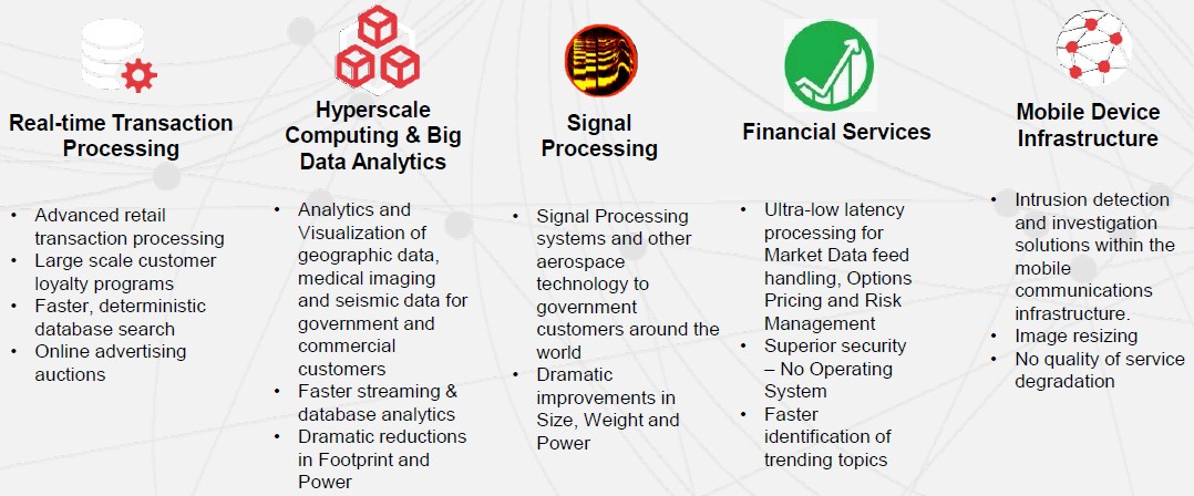
The first is that customers can program their hardware to behave any way they want and to have the features – and only the features – they need. If you need 50 floating point units on your system, that is what you put on them. Also, because the application and its dataflows are implemented in HDL and essentially running as hardware, you get deterministic performance. Every time you run a routine, it behaves the same exact way. (You can’t say that about a general purpose CPU juggling many things.) Moreover, the FPGA can change its personality on the fly, allowing for mixed workloads on the hybrid nodes over the course of a day. (It takes about a second to change out the application personality on the FPGA, according to Huppenthal – not quite fast enough for context switching speeds inside of applications, but a lot faster than firing up a virtual machine and a whole lot faster than configuring a bare metal server by hand.) Because the FPGA only does the work the application requires (again, the application is the processor), and it executes portions of the code in parallel, the FPGA has a very high utilization rate and, as it turns out, very low power consumption. The combination of high parallelism and low power are what enables a massive amount of potential server consolidation for all kinds of workloads in a datacenter. There are a plethora of use cases for SRC to chase:
This energy efficiency of compute is also, as it turns out, what allows SRC to create signal processing and control systems that can fit inside of a drone, systems that cannot be created given the performance and power draw of traditional, general purpose CPUs. So MAP and Carte are not just a science project, but technology that has been literally battle-tested in the field. And, importantly for financial services, defense, intelligence, and other customers who have FPGA applications already, Carte will allow existing Verilog and HDL code to run on the MAP hybrid processors and be called as routines.
Saturn 1 Takes A Moonshot
SRC has been building ruggedized rack and mobile servers for the military and intelligence communities for a long time using its MAP hybrids, and it even has a homegrown crossbar interconnect switch called H-Bar that can be used to lash multiple MAP nodes together into clustered systems. But to attack the hyperscale market, SRC decided to partner with Hewlett-Packard and create a MAP cartridge for HP’s Moonshot hyperscale system.
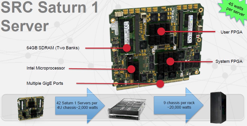
The Moonshot machines were launched in April 2013 and started ramping as that year ended. The machines have a very compact architecture and offer a lot of compute density, but given that the “Gemini” Moonshot chassis comes in a 4.3U form factor and has 45 compute nodes, you can’t put a very beefy processor on each cartridge, and that limited their appeal in many datacenters. You can, however, put four fairly small processors on a single cartridge, which makes for interesting use cases. Or, as it turns out, you can put on an Intel Atom processor and two Altera Stratix IV FPGAs, as SRC has done to create its Saturn 1 server node:
The interesting bit about the Moonshot machine, explains Eaton, is that the backplane in the chassis has a backplane that implements a 2D torus that has 7.2 Tb/sec of aggregate bandwidth. This interconnect can be used to link all of the nodes in the chassis together (they can be compute or storage nodes) without the need for any additional switching. The two switch modules in the Moonshot chassis are for linking the nodes to the outside world, which can be additional Moonshot enclosures or the upstream network that links to users and other applications. This 2D torus interconnect can link three nodes together in a multiple-tier, as is common for many applications that are based on web, application, and database tiers, or can hook up to fifteen nodes together in a relatively tight cluster that is more akin to the kind used in modeling and simulation applications in the HPC realm. The point is, by switching to the Moonshot enclosure, SRC doesn’t have to use its Hi-Bar interconnect to link machines together.
While the Moonshot system is an elegant and clever design, it has not been a barn burner for HP, and part of the reason is that there is limited appeal for the compute elements that can be put on a single cartridge. As to that, Eaton says: “We may be the cartridge that the Moonshot chassis has been waiting for.”
The Saturn 1 cartridge has a four-core Intel Xeon Atom processor on the X86 side and two Altera Stratix IV GX530s on the FPGA side. One of the FPGAs implements the SNAP interconnect and multiple virtual Ethernet ports that are used for the 2D torus interconnect and to link to the HP switches in the Moonshot enclosure. In most cases, SRC’s early customers are putting a compute node in each row of cartridges and using that as a Linux boot engine from which data gets fed into the remaining 42 MAP hybrid nodes in the enclosure. The MAP nodes do not run an operating system – it is not necessary since the nodes, by design, directly run application code – but customers can boot a Linux kernel on each Atom processor if they want to, according to Eaton.
SRC is charging $19,950 per node for the Saturn 1 cartridge, and that includes the bootloader code required by Intel and Altera for their respective Atom and Stratix processors as well as a license to the Carte environment. Volume discounts obviously apply. But given the kind of consolidation that SRC is projecting for its workloads, customers might not be buying very many of them.
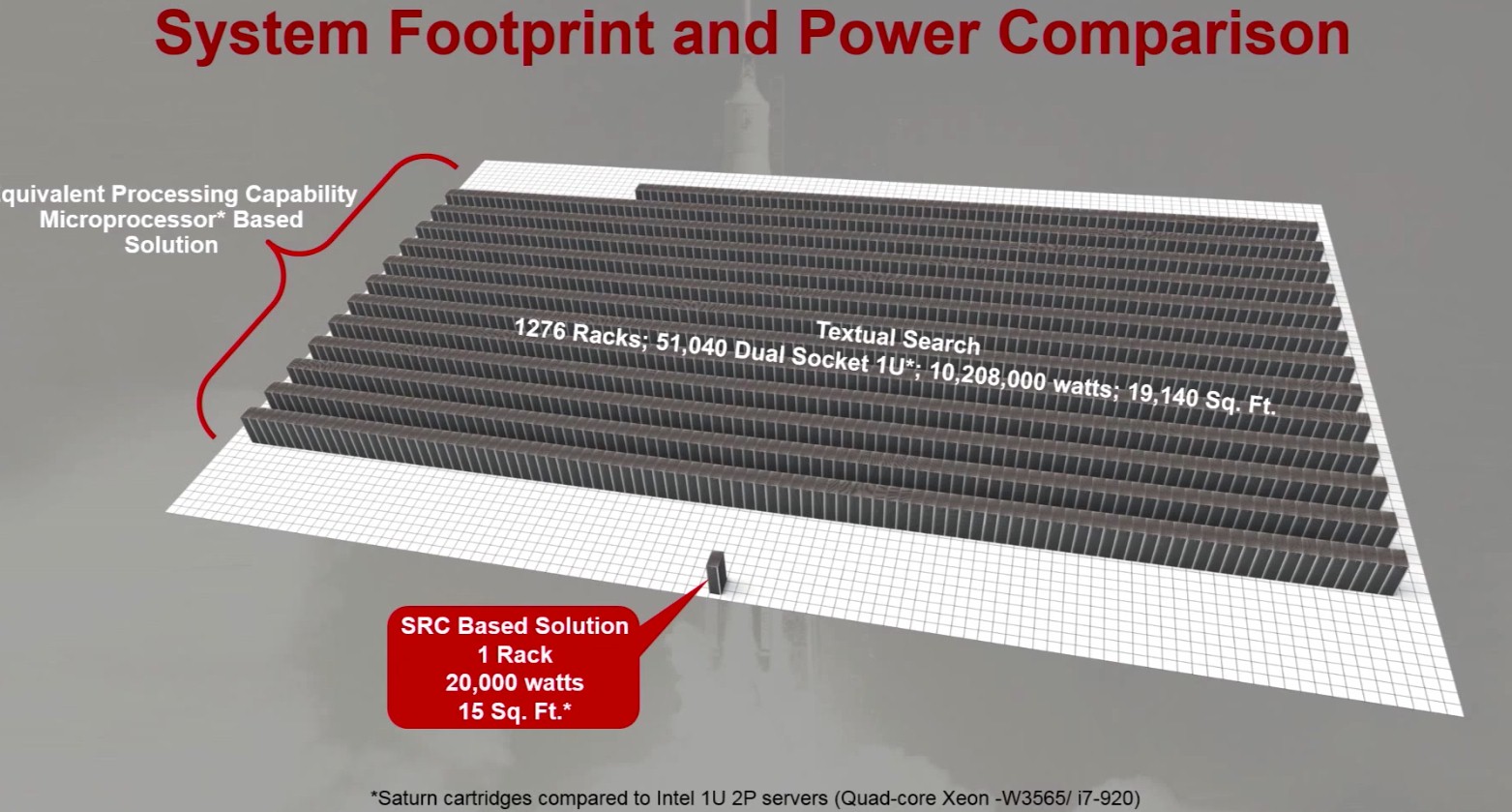
In his presentation, Huppenthal ran some text search benchmarks on a Saturn 1 node and a two-socket server using a high-end quad-core Xeon W3565 workstation processor. (This one has a 3.2 GHz clock speed.) Based on the benchmark results, it would take 1,276 racks of these two-socket servers to do the same work as a rack of Moonshot systems equipped with nine enclosures and a total of 378 MAP hybrid processors. That is a total of 51,040 server nodes and 408,320 cores on the Xeon side and over 10 megawatts of power. The kind of thing you might see at the National Security Agency, for instance.
This comparison is a bit unfair, since those Xeon W3565 processors date from 2009, back in the “Nehalem” days. The compression is not really 1,276 to 1. (And SRC knew that when it made the comparison, obviously.) If you built a cluster using two-socket machines based on the latest “Haswell-EP” Xeon E5-2667 processors, which have eight cores running at 3.2 GHz and considerably more instructions per clock than the Nehalem Xeons did, you would need about 314,406 cores to do the same work, and if you do the math, that would be 19,650 nodes. If you had dense pack, four-node hyperscale machines, that would work out to 234 racks of X86 iron, not 1,276 racks. That is still a huge number of cores, it would still be several megawatts of power, and it is still a huge compression ratio for this text search example if the Saturn 1 performs as expected.
In general, what SRC is saying is that across a wide range of applications that can be accelerated by FPGAs, customers can expect to get around 100X performance with 1 percent of the energy consumption, 1 percent of the footprint, and at under 25 percent of the cost of equivalent performance for X86 server clusters.
More Compute Oomph And Lower Latency
SRC trotted out one of the early customers for the Saturn 1 hybrid server node, an advertising startup called Jingit that is based in Minneapolis, Minnesota and that is prepping its first product to come to market later this year. The company was, as most hyperscalers do, building its stack on X86 clusters, but the nature of the service it is providing made Jingit take a stab at using the SRC system. (SRC has a development lab in the area, so somebody clearly knows somebody here.)
What Jingit wants to do is provide consumer marketing services at the point of sale, which in plain English means kicking out a custom coupon to you as you are buying something. The difficulty is that their backend system has to come up with whatever deal is appropriate for you, based on this current purchase and past purchases, in somewhere around 50 milliseconds to 130 milliseconds, which is the time it takes for a credit card authorization to occur. It was taking a lot of iron to make this happen on the X86 architecture, which was bad, but the total processing time was the real problem.
Including the inbound and outbound message time on the credit card networks, the processing time to be at the current industry benchmark rate should be around 50 milliseconds, with the spare time to compute anything being a very small fraction of that – single digit milliseconds. But the processing time on the X86 clusters was pushing the total transaction time to around 1,500 milliseconds. And 1.5 seconds in our impatient world is a lifetime, apparently. Running the same application on the Saturn 1 nodes, the calculations were being done in nanoseconds, and the response time was quicker than the jitter in the credit card network. Todd Rooke, one of the co-founders of Jingit, says that it is not possible to measure the speed it is happening so fast and the speed of the credit card networks is so variable.
SRC has been attacking various markets where you would expect to see FPGA acceleration for many years, but the difference this time around is that with the combination of the Moonshot chassis and its more sophisticated Carte programming environment, the whole shebang is perhaps a little easier for prospective customers to consume.




This board is based on devices that are 2 generations behind and, at $20,000, it’s 10x too much money. SRC would have gone out of business if the government had not propped them up for years. When Cray died the New York Times wrote and article about how he “invented” reconfigurable computing. I already had patented issued by the time he started his company. In fact I have the patent on CPU-FPGA hybrids (http://1.usa.gov/1FrPbJk). I have the first paper on reconfigurable computing as it’s defined today http://commacorp.com/First_contract.pdf. My products replaced OctigaBay hardware at Cray and Cray OEMed equipment that I designed and manufactured.
Burroughs was selling reconfigurable computing in the 1970s. Intel tried too with the Itanium … which officially is still alive, I guess. The whole CISC computer architecture going back to the IBM 360 and governed by microcode, is basically reconfigurable computing. It’s described in Turing’s 1936 paper that invented computing. Have a nice day.
That was the B1700. WAY ahead of its time. Can’t get a 8080 in your hands ? No problem have the B1700 run as one (Did that while at Big B). Need to tweak how Fortran does something ? Change or add to the microcode.
Good architecture to read up on
-pete