


One of the oldest adages in the systems business is that customers don’t buy processors, but rather they buy roadmaps.
The trick with being a server compute engine supplier – whether you are talking about CPUs, GPUs, or any other kind of device – is to reveal enough of the roadmap for the product line to convince people you really do believe in the product, but not so much that you give away competitively damaging information to your rivals. In the case of Intel, its increasing number of rivals as it expands its compute engine portfolio at the same time that more rivals take a run at it.
Given where Intel is at in the datacenter today, with its Xeon SP business under attack from AMD’s Epyc X86 server chips and the Arm collective, led by Amazon Web Services and Ampere Computing these days, making some headway into the glasshouse, particularly among big hyperscalers and cloud builders, you would think that Intel would publicize a roadmap with a general description of the innovations it will bring to bear and the timeline for doing so.
Intel is an underdog when it comes to credibility with compute engines, which is hard to believe sometimes but it is true nonetheless. Intel’s chip manufacturing technologies not only ceased to advance in a way that is competitive with industry juggernaut Taiwan Semiconductor Manufacturing Co, but the constant delays in process technologies wreaked havoc on its planned CPU rollouts. Moreover, Intel dragged its feet on chiplet architectures at a time when AMD innovated first with its initial Epyc processors in 2017 and has perfected in the follow-on two generations of X86-compatible server chips. AMD is now setting the technology pace, and has a foundry partner that is helping it to do this on the CPU, GPU, and soon the FPGA fronts once the Xilinx acquisition clears within this quarter or so.
Under these circumstances, and given that chief executive officer Pat Gelsinger has been at the helm for over a year now, you would think that Intel would do precisely what Oracle co-founder Larry Ellison did after acquiring Sun Microsystems in January 2010: put out a five-year roadmap that said something, and then stick to it. AMD did the same when it came back into the server space with the Epycs in 2017, and continues to do now to a lesser extent.
The problem, we think, is that Intel itself is not sure of its own future, even a year after Gelsinger came back to the company and took the helm of the chip maker, and perhaps the person who could have prevented all the chaos if he was not passed over for the job back in September 2009 as the Great Recession was roaring and Intel’s hegemony in the datacenter was nearly complete. After being back six months, Gelsinger reorganized the company, creating new business groups and empowering new executives, but make no mistake: Gelsinger is in charge of the whole Intelchilada, with a side order of chips with queso.
With rumors running around that the next-gen “Sapphire Rapids” processors were going to be pushed into the third quarter – something that Intel people denied when we asked about it this week – we started poking around the rumor mills for the Xeon processor roadmaps, much of which is encapsulated in a video posting by Tom (Last Name Unknown) of the Moore’s Law Is Dead blog and also of the Broken Silicon podcast. If you surf around the web, you will find all kinds of sites that are pointing to this post on MLID, and there have been lots of other things rattling around since last summer about how the Intel chip roadmaps for 2023 and beyond have been changing. While this is all interesting, what we want to know is what the future of the Xeon server might look like, and how this might affect the applications and the market of that future. Most applications in the world are still doing most of their compute on CPUs, so what happens on the server CPU matters most to most of the world.
And so, to get a handle on what is potentially coming down the Xeon pike from Intel and what effect it might have, we have built a series of tables that show where we went from “Sandy Bridge” Xeon E5s to “Cascade Lake” Xeon SPs for two-socket machines and then separately projected out from “Ice Lake” Xeon SPs from last year to “Diamond Rapids” Xeon SPs – if Intel still intends to call them that – expected in 2025 and maybe 2026, depending on how it goes.
This is as much to organize our thoughts as anything else.
As usual, items shown in bold red italics in the tables are estimates for those features in the absence of data, and it is based on expected generational improvements in signaling and clock rates for various features and reasonably anticipated capacity increases based on transistor density, energy consumption, and chiplet architectures. And to be fair, in many cases, Intel does not yet know what these future Xeon SPs will look like because there is still a lot of engineering to do to bring PCI-Express 6.0 peripheral controllers or DDR6 memory controllers to market and the CPUs have to intersect the availability of peripherals and memory to plug into these controllers.
Our tables ignore single-socket, four-socket, and eight-socket platforms and the tweaks to the Xeon CPUs that are necessary for them to be created. These systems represent maybe 20 percent to 25 percent of the volumes in the market and about the same share of the money, and the tweaks to create chips and chipsets for them are fairly modest. Different numbers of cores and different numbers of QPI or UPI links are needed to be activated in the chips and chipsets, but the underlying architecture stays, relative to each scale of the server node, changes more or less in lockstep.
Let’s take a look at the legacy Xeon E5 and Xeon SP platforms first to get a full feel for the levers that Intel has to play with as it has advanced CPU compute, memory and interconnect between 2012 and 2020:

In each case, we are looking at the top of the line part in each generation of Xeon E5 and Xeon SP, which is often called the top bin part in the chip industry. This is the variant of each generation that has the most cores and pushes the thermal limits as high as they could go for systems of that generation.
As you can immediately see, there are a lot of different levers that Intel has pulled – and having the manufacturing process lever stuck at 14 nanometers from 2016 through 2021 obviously made the Xeon chips larger and more expensive to manufacture and also caused Intel to hold back core count and actually reduce cache. Clock speeds also took a dive for a while to help pay for the thermal room to increase core counts while not moving on to the much-delayed 10 nanometer manufacturing processes at Intel. And instruction per clock (IPC) improvements, normalized for a constant clock rate and a single core, also were not often impressive. “Cascade Lake” Xeons were really “Skylake” Xeons with a few different instructions, and with the Cascade Lake-R refresh in early 2020, when AMD was starting to get traction bigtime with its “Rome” Epyc 7002 processors, Intel rejiggered the two-socket Xeon SP-6200 series Gold variants and chopped the hell out of prices after taking huge profits out of the Skylake line ahead of AMD’s Epyc ramp. (We discussed how high the relative price of the Skylakes were to the prior Xeons in The Huge Premium Intel Is Charging For Skylake Xeons back in September 2017, showing it was clearly profit taking.)
This was not the first time in the history of server chips from Intel that the company did this. “Haswell” Xeon chips from 2014 offered slightly worse bang for the buck in terms of raw throughput performance than the “Ivy Bridge” Xeon E5s they replaced (at least for the top of the line chips), and Ice Lake Xeon SPs cost slight more than the Cascade Lake-R Xeon SPs, too, but a lot less than the original Cascade Lake Xeon SPs from 2019. But the Skylake chips set a high water level that Intel can never return to. At list price, Intel offered half the bang for the buck with the Skylake CPUs as it did for the “Broadwell” CPUs that preceded them. This is what happens when you have no competition. And to be perfectly fair, there was a 58.5 percent increase in throughput between the machines, which is worth something. (That relative performance is the product of IPC change, core count, and clock speed as gauged against the four-core “Nehalem” E5500 processor from March 2009, which is how we have been reckoning this since The Next Platform was established seven years ago.)
To make the Skylake and Cascade Lake processors valuable to datacenters, AVX-512 vector engines and a second generation fused multiply add (FMA) unit were added to the Xeon cores, and PCI-Express controllers got more lanes (even if they did not get faster), memory speeds inched up across the generations, and so did QuickPath Interconnect (QPI) links; more links were also added to more tightly couple NUMA nodes with two, four, or eight processors. The wattages of the devices also crept up because as everything runs a little faster, it runs a more than a little hotter at an exponential rate.
Balancing all of these pressures in a CPU design is a serious challenge, and Intel chip designers have had one hand tied behind their back and the other one with a fat space glove on because Intel’s foundry was not able to get 10 nanometer, 7 nanometer, and 5 nanometer ticks out the door in a timely fashion to interleave with their architectural tocks.
It has been painful to watch, to be frank, and very frustrating for datacenter customers who need to maximize performance per dollar per watt, always.
With the “Ice Lake” Xeon SPs that came out last year, we saw what could have been back in 2017 or 2018 finally realized in a 10 nanometer process, and the Ice Lake chips lay the foundation for what looks to be a roadmap that has an annual cadence (more or less), server platforms that span two generations of Xeon SPs, and what promises to be a impressive ramp of compute, memory, and interconnect as well as a healthy dose of generational IPC improvements to go along with expanding core counts that chiplet architectures enable in a server CPU socket.
At its Architecture Day last summer, Intel provided some of the salient features of the “Sapphire Rapids” Xeon SPs coming out this year, which are slated to plug into the “Eagle Stream” server platform. As far as we know, there is not going to be an “Advanced Platform” variant of the Xeon SP platform that crams two whole processors into a single socket, as happened with the “Cascade Lake-AP” variants from 2019. But there are rumors about an AP platform called “Birch Stream” coming out with the future “Granite Rapids” and “Diamond Rapids” processors due in 2024 and 2025, respectively.
The Granite Rapids doubled up variant is reportedly called “Sierra Forrest,” and is like the “Bergamo” variant of AMD’s Genoa Epyc 7004 processors, aimed at hyperscaler and cloud customers who want the maximum number of cores in a socket they can get. The point is, even with the massive core counts we are projecting, Intel seems like it is going to be doubling them up inside a package. IBM is doing this with Power10 this year, too. This is not a new idea, but rather a very old one dating back to the Dot-Com Boom, when IBM, Hewlett Packard, and Intel all put DCM variants of their server chips into the field to increase compute density in their servers.
For the purposes of our comparisons of future Xeon SP processors, we are ignoring these AP variants as well as those that will employ HBM memory to boost memory bandwidth for the processors. These are important, and so will other variations on a theme such as packages that include various kinds of accelerators while others do not. There is going to be a kind of mass customization going on in compute, and as we have pointed out before, this will mean that volumes will go down for any specific variation relative to the volumes on a much more streamlined product in the past. There was one and only one Nehalem Xeon CPU, with some features activated or not. In a chiplet architecture world, all kinds of variations will be possible – and probable. We also think that Intel will eventually do a mix of big and little cores – what it calls P core and E cores, short for performance and efficient – in servers, and we are ignoring how this might play out and are looking at chips with only P cores in the future Xeons.
So here is our best guess at what the next four generations of Xeon SPs will look like compared to the current Ice Lake Xeon SPs:
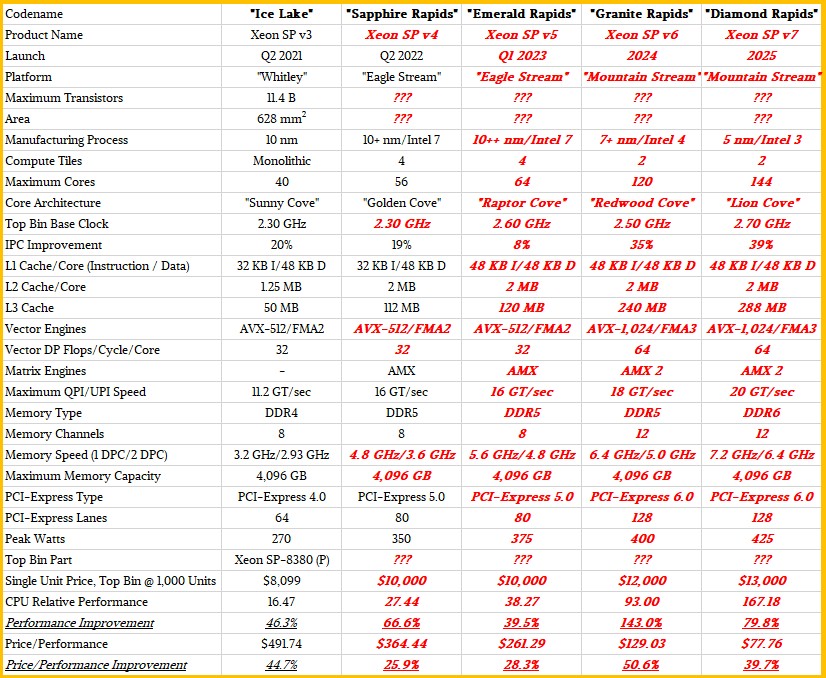
As we have said, anything in bold red italics is a guess on our part. It is as much a template against we will judge what Intel actually does as it is an attempt at predicting what Intel might do.
We think that the future “Emerald Rapids” Xeon SP due around a year from now and a kicker upgrade for the Eagle Stream platform, is a full-on variant of Sapphire Rapids with all of its cores activated (or new chiplets for the core complex) and faster DDR5 memory. Given the core count, clock speeds, and IPC improvements, we expect the top bin 56-core Sapphire Rapids chip will have around 67 percent more throughput than the top bin 40-core Ice Lake chip, and we think further that Intel will raise the price on the chip to around $10,000 and deliver around a 26 percent better bang for the buck.
Which brings up a good point. Of all of the levers that can be pulled, price is the biggest lever and the easiest one to yank very hard. If AMD or the Arm collective gets aggressive in terms of performance or price – or both at the same time – then Intel will have to follow suit. We expect for everyone to try to get more money per chip and to cram more oomph into each chip to justify the higher price. These chips will be more expensive to make, so why not?
We expect for the top bin Xeon SPs to get more expensive, and that is because we expect that the incremental compute they are offering with each generation is going to be, compared to the past ten years of the Xeon line, truly astounding.
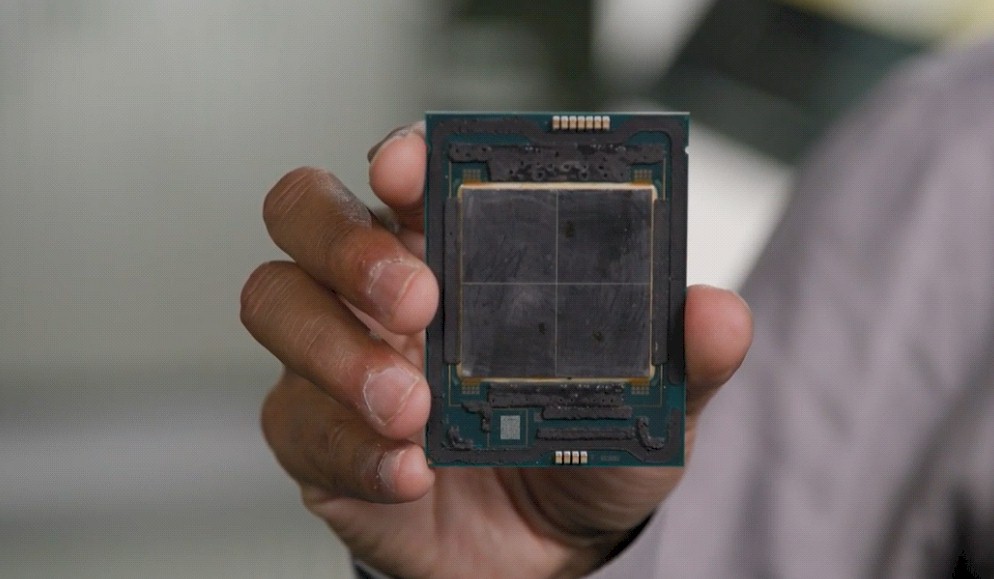
Granite Rapids and its kicker, Diamond Rapids, are a good case in point. At last year’s Intel Accelerated event, the chip maker put out a die shot mockup of Granite Rapids, which we show in the feature image at the top of this story and which we repeat here:
![]()
This mock up shows two central blocks of core tiles, each with 60 cores, surrounded by what could be HBM and cache memory or PCI Express and memory controllers. (We think it is the latter, not the former.) To compete with AMD Epyc chips, Granite Rapids is going to have to have around 120 cores, so maybe Intel just put an Easter egg in its presentation for fun.
One of the rumors going around is that the “Lion Cove” core that will be used in the Diamond Rapids Xeon SP chip will have twice the IPC as the “Golden Cove” core used in Sapphire Rapids CPUs.
Here is a chart that plots out IPC improvements over time compared to the “Dothan” Core architecture that saved Intel’s cookies from AMD during the Opteron generation:
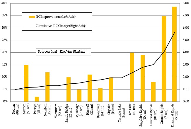
This 2X IPC jump between the Golden Cove and Lion Cove cores seems like a difficult thing to pull off, but the table above gets that 2X IPC and shows the performance and price/performance of the resulting processors. The expectation is that the IPC in the “Raptor Cove” cores in the Emerald Rapids Xeon SPs will have between 5 percent and 10 percent IPC improvements over the Golden Cove cores used in the Sapphire Rapids Xeon SPs, and we just show it at the midpoint of around 8 percent. To make that 2X jump, the Redwood Cove and Lion Cove cores used in the Granite Rapids and Diamond Rapids Xeon SPs, respectively, need to deliver the biggest IPC improvements in Intel’s history.
If Intel can do that, and etch the cores in decent processes (of its own or those of TSMC), and cram as many cores as we show into a package, then the mainstream Xeon SP chips of 2024 and 2025 could be truly impressive. If it all plays out as we expect, a top bin Diamond Rapids processor will cost 6.3X of a top bin Sandy Bridge Xeon E5, but have 18X more cores, deliver 65.6X more throughput performance, and drop the cost of a unit of performance by 90.4 percent.
Such changes would utterly change the nature of CPU compute in the datacenter. Even if Intel doesn’t do this, it looks like AMD and the Arm collective can and probably will. We strongly suspect that it may take another generation or two for Intel to reach its apparently lofty goals. We shall see.