


AMD is hosting its “Next Horizon” datacenter event in San Francisco this week, and archrival Intel, which is losing some market share to AMD but not feeling the pain on its books yet thanks to a massive buildout in server infrastructure at hyperscalers, cloud builders, and smaller service providers like telcos, is hitting back by divulging some of its plans for next year’s “Cascade Lake” Xeon lineup.
If all goes well, AMD is going to be first to market with a 7 nanometer chip when the Rome Epycs debut next year, and with Intel having bigtime issues that won’t see it deliver its “Ice Lake” Xeons until early 2020 in volume, Intel has to do something. And that something is to mimic what AMD is doing, and as it has done itself when under pressure from AMD in the server space in years gone by, and that is to cram two whole processors into a single socket to jack up the core count and memory controllers with the Cascade Lake Advanced Performance chips, or CLX-AP for short in the Intel lingo.
Lisa Spelman, general manager of Xeon and datacenter marketing at Intel, prebriefed the press on some of the details about the Cascade Lake AP processors ahead of the AMD event, and it is clear that Intel wants to be a spoiler and make everyone think twice about the Epycs. We covered the future roadmap for Xeons – including the Cascade Lake, Cooper Lake, and Ice Lake chips due in the next two years – in detail here and went into the standard, single chip module (SCM) variants of the Cascade Lake there. So we are not going to repeat all of that again, except that Intel is going to try to counter AMD’s Rome chips based on 7 nanometer chip making processes with the Cascade Lakes etched from refined 14 nanometer processes.
This is not the first time that Intel had to cram two Xeons into a socket to take on AMD. Way back in October 2005, in the wake of AMD getting the first dual-core Opteron X86 server processors to market (based on a monolithic design), Intel cooked up the “Paxville” Xeon DP chips, its first multicore module (MCM) implementation in the Xeon line and clearly a stop-gap measure at the time. Having MCMs is not a stop-gap anymore, but really the only practical answer to trying to put more cores into a socket without having the price of the chip and its thermals go through the roof. The thermals for the Cascade Lake AP Xeon might go through the roof just the same, if history is any guide.
To make a “Naples” Epyc 7000 series processor, AMD takes an eight-core Ryzen chiplet with two memory controllers and uses some PCI-Express 3.0 interconnect lanes to create an “Infinity Fabric’ that lashes them together to present themselves as a very tightly coupled baby NUMA server in a socket with 32 cores and eight memory controllers. Other PCI-Express lanes are available to be used as I/O or to create a two-socket chip.
Intel is not precisely doing this. Rather, it is taking a future Cascade Lake part with three UltraPath Interconnect (UPI) links that are used to link multiple servers into various NUMA topologies and cross-coupling the two chips together so it creates what looks, to the outside world, like a 48-core socket with twelve memory controllers on it. Like this:
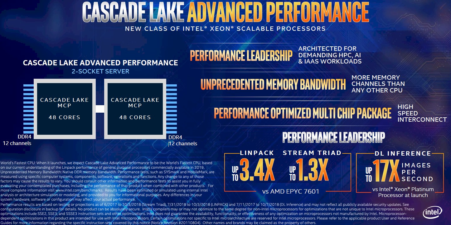
Intel has taken a beating in some regards because its top-end “Skylake” Xeon SP-8180M Platinum chip, which packs 28 cores on a die, burns at 205 watts and only has six memory controllers. So the AMD Epycs as well as the Cavium ThunderX2 and IBM Power9, have a 33 percent advantage when it comes to memory capacity and memory bandwidth. These monolithic Skylake Xeon chips are also expensive compared to prior generations of Xeon chips, and probably have relative bad yield even if they are made on refined 14 nanometer processes that are getting pretty mature because they are such large chips. Intel can’t really cram more cores on a tie when it is stuck at 14 nanometers, hence the MCM.
In this case, the MCM will have two 24-core dies, each with the six memory controllers like the Skylake dies have. There is not one Skylake Xeon SP processor, but rather three different ones, and we think the die layout will remain essentially the same for Cascade Lake SP chips, which we know top out at 28 cores. (Intel has added some performance enhancements, hardware mitigations against the Spectre/Meltdown speculative execution vulnerabilities, and the VNNI deep learning acceleration instructions with Cascade Lake SPs.) The LCC variant of the Skylake and Cascade Lake Xeons has up to 10 cores on a mesh interconnect, the HCC variant has up to 18 cores, and the XCC variant has up to 28 cores. So it looks like Intel is taking something akin to the 24-core Xeon SP-8160M, which runs at 2.1 GHz and which costs half what the top-bin Xeon SP-8180M with 28 cores running at 2.5 GHz costs, and gussying it up with those extra Cascade Lake features and then popping two of them in a single socket.
“It is our intent and design to deliver performance leadership throughout 2019,” says Spelman. Ah, but you can never forget about price or about thermals, which Spelman did not mention. This is probably not an oversight on Spelman’s part, since the MCM version is probably going to have to gear back clocks to cram two 24-core chips into a single socket. And even then, this could end up being a 275 watt or maybe even a 300 watt or 350 watt part. (It all depends on the clock speeds chosen.) So Intel could meet or beat AMD on performance, slash prices like crazy (with this 48-core Cascade Lake AP part not costing much more than a monolithic top-bin 28-core Skylake part), and still lose out bigtime on performance/watt and cost/performance/watt.
Everyone has the physics and thermodynamics concepts here. “For those who are power constrained, we have options,” says Spelman. “And for those who are performance constrained, we have options.” Just like during the Paxville Xeon days, which were a stopgap until Intel could get true dual-core monolithic dies out the door a year later.
This is sounding very familiar, only this time the rush is to perfect MCMs. They are now a given, thanks to the slowing down of Moore’s Law.
We have little doubt that using that third UPI link coming off each Cascade Lake XCC die to cross couple the two chips on the Cascade Lake AP package will have a performance advantage compared to the current Naples Epyc 7000s, since the UPI links have more bandwidth and lower latency than PCI-Express 3.0 lanes and because there are only two chips in the socket (one hop either way) compared to the Naples chiplets, which are either one or two hops away from each other, depending.
This two-chip Cascade Lake AP module will, says Spelman, offer up to 3.4X the Linpack double precision matrix math performance of a 32-core Epyc 7601 from Intel, and will deliver 30 percent more memory bandwidth performance based on the STREAM Triad memory bandwidth test. Considering that there are 50 percent more memory controllers on the Intel chip than on the AMD chip in this comparison, it looks like Intel has to slow the DDR4 memory controllers and the DDR4 memory sticks down a bit to save power. Separate from the chart above, Intel tells The Next Platform that the 48-core Cascade Lake chip will have 21 percent more oomph on Linpack than the top-bin Skylake Xeon SP-8180M Platinum chip with 28 cores running at 2.5 GHz, and if you do some rough math, that puts the clock speed of the Cascade Lake AP at around 1.8 GHz. On the STREAM Triad test, the future Cascade Lake AP MCM will beat the top-bin Skylake Xeon SP SCM by 83 percent, which is pretty good, but will only be 30 percent better than the AMD Epyc 7601.
The Cascade Lake SP and AP chips will come out all at the same time, which is during the first half of 2019 – about the same time AMD will roll with the Rome Epycs – if Taiwan Semiconductor Manufacturing Corp doesn’t hit any snags with its 7 nanometer processes.
We will see what AMD has to say this week out in San Francisco, and then take stab at trying to figure out how it will map to what Intel is doing. We have heard on the rumor mill that Rome Epycs will have 48 cores (as we expected) and only eight memory channels (we were hoping for more, but Rome has to be socket compatible with Naples); others are expecting AMD to crank Rome up to 64 cores in a socket, and still others say Rome is 48 cores and the kicker “Milan” processors will reach up to 64 cores. Intel just forced AMD’s hand into disclosure.