


Two decades ago, all the chip makers, including Intel, had to buy Unix machines, usually massive ranks of Sparc/Solaris systems, to do electronic design automation to design and test their chip designs. Intel coveted that server business, and at the same time caught the Linux bug and obviously had a strong motivation to move EDA to X86 platforms.
But Synopsys, Cadence, Mentor Graphics, and others were having none of that heavy lifting. So Intel, in a fury of enlightened self-interest, helped them all port their EDA tools to Linux on X86. It was a huge effort, and it was wildly successful in helping to drive the cost of the computing, inside the datacenter and out, down by making design a lot cheaper and therefore more scalable.
We may be seeing an equally dramatic transformation of chip design right now, this time with the use of AI to drive designs.
It wasn’t that long ago, back when Moore’s Law was more the principle of how things in the semiconductor business worked and was less an academic debate of whether or not it is dead, moving from 45 nanometers to 32 nanometers to 28 nanometers to 22 nanometers to 16 or 14 nanometers on down to even 10 or 7 nanometers, while challenging, was eminently doable.
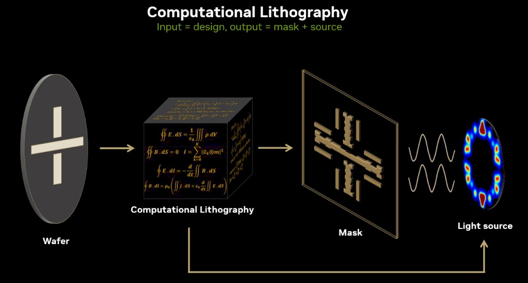
Now Intel, AMD, and others are hitting – or aiming for – 5 nanometers, 3 nanometers and are pushing to 2 nanometers and even 1.8 nanometers and smaller transistor geometries. The old ways of doing things are essentially impossible at that scale, and semiconductor manufacturers turning to computational lithography to efficiently get chips onto wafers using algorithms to simulate production operations and to create masks for fabrication, which Nvidia founder and CEO Jensen Huang described at the recent GPU Technology Conference as an “imaging problem at the limits of physics.”
“Each chip design is made of about 100 layers, and in total contains trillions of polygons these days or patterns,” Vivek Singh, vice president of Nvidia’s Advanced Technology Group, told reporters and analysts during a virtual meeting describing Nvidia’s GPU-accelerated lithography. “Each of these hundred layers is encoded separately into a photo mask, a stencil for the design, and using a rather expensive camera, is successively printed onto silicon. This creates a three-dimensional structure made of transistors and wires forming a chip.”
Singh added that about 30 years ago, “the transistors and wires that make up chips shrunk to where they were even smaller than lasers used in cameras, creating diffraction and blurring the image of the transistors. The image would have gotten more and more blurred and nothing would have printed if we didn’t do anything about it. Something had to be done to bridge what is called the wavelength gap. That something is computational lithography.”
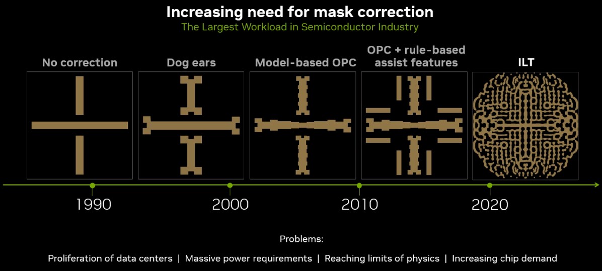
All this is drives up the need for compute. Smaller transistors mean more complex calculations, which for datacenters translate into more servers dedicated to computational lithography. The number of these datacenters is growing at a faster rate than Moore’s Law, so that a silicon fab that uses three datacenters now will need 100 datacenters by the end of the decade, he said. “If the trend of the last 15 plus years continues for only a few more years, that’s not feasible.”
A lot of effort is going into creating tools to more easily enable computational lithography to keep the wheels of efficient, fast, and cost-effect chip making turning. As Intel did earlier with X86, Nvidia is now doing the same enlightened self-interest, only this time it is using ultraviolet rather than visible light. Thus the introduction at the recent GTC 2023 event of cuLitho, a computational lithography software library that is designed to run on the GPU-maker’s DGX H100 supercomputers powered by its “Hopper” H100 GPU accelerators.
Nvidia is making the same argument with cuLitho that it has made since pushing its GPU accelerators in into the datacenter well over a decade ago – that shifting highly parallel-processing workloads (like, in this case computational lithography) from the CPU to the GPU can greatly improve performance as well as efficiency.
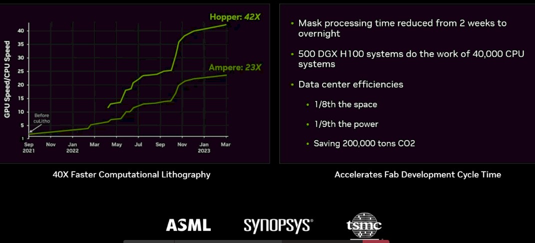
Nvidia says that the combination of cuLitho, DGX systems, and Hopper GPUs can mean a performance jump of more than 40X at a fraction of the power – from 35 megawatts for CPU-powered systems to 5 megawatts using Nvidia’s iron. Using cuLitho, fabs can produce 3X to 5X more photomasks with 9X less less power than what is done now. Processing for a photomask that typically requires two weeks can now be done overnight, according to Nvidia. Nvidia calculates that 500 DGX systems that hold 4,000 H100s and leverage cuLitho for computational lithography jobs will match the performance of 40,000 CPU-powered systems while consuming 1/7th the energy.
The library also will run on older Nvidia GPU architectures, such as Volta and Ampere, though those companies starting from scratch should do so with Hopper.
Nvidia is getting some industry players behind its efforts. Taiwan Semiconductor Manufacturing Co. is integrating cuLitho into its foundry operations, equipment maker ASML will integrate support for GPUs into its computational lithography software products, and EDA company Synopsys bringing cuLitho into its software and systems.
All that said, there are still details of cuLitho that Nvidia isn’t talking much about, including business models – such as who will license it, whether it’s EDA vendors or customers – and Singh deflected a question about AI and cuLitho, saying the vendor isn’t saying to much right now about the algorithms being used. However, he added that “AI is very much in the works in cuLitho. We are at 42x [with performance improvements over CPU-based systems]. I expect on with the help of AI to actually speed things further.”
That’s not surprising. AI is quickly making its way into the layout and design of semiconductors. As we recently wrote, Nvidia last month laid out how to use its four-year-old DREAMPlace GPU-accelerated deep learning toolkit to determine how to place macros – transistor blocks such as memory, analog devices like PCI-Express controllers or memory controllers, or the cores themselves – on a semiconductor device, accelerated what is typically a highly manual process.
Synopsys is going all in on AI with its EDA tools. In 2020, the company took the first step in that direction, introducing DSO.ai, an AI-infused application for chip design that earlier this year hit a milestone by reaching 100 production tape outs. Companies like Samsung and Microelectronics use DSO.ai and Synopsys used the tool to test out AI in one of the various steps in the chip design process. It was the proving ground for the company, according to Arvind Narayanan, senior director of product line management for Synopsys’ EDA Group.
“How do you use AI effectively to build models to get to that global minimum much faster than humanly possible?” Narayanan tells The Next Platform. “That was the first foray for us. We have learned quite a bit from that.”
Initially it was used by organizations for optimizing power, performance, and area (PPA) in their semiconductor designs. However, since then designers have expanded its use to include determining the best configurations for flow planning and accelerating the migration from one design to another.
At its recent Synopsys User Group (SNUG) event late last month, the company rolled out Synopsys.ai, essentially adopting AI and machine learning technologies into every part of the EDA process, housed under three categories – DSO.ai (Design Space Optimization), VSO.ai (Verification Space Optimization), and TSO.ai (Test Space Optimization), for design space, verification space, and test space optimizations. It all touches on everything from silicon manufacturing to implementation to system architecture, with much of that being informed by what the EDA vendor learned through DSO.ai.
“Once you scratch the surface of implementation with AI and you see that it’s helping significantly more from a productivity angle and PPA, the next immediate question was, what are you doing about adjacencies,” Narayanan says. “If you have AI working for implementation, what about verification, what about test, what about signoff? There’s a lot of steps in each of these floors. Next, how can you use … the models that are being built? How can you share that across the floor and how can you use that effectively? As we moved along, we uncovered use models and customers started asking us why is this only one piece of the puzzle that you’re looking at? It needs to be the solution. That’s when we started expanding and looking at opportunity limits.”
As with Nvidia’s move with cuLitho, the Synopsys.ai strategy is driven by the increasing complexity as the manufacturing processes get smaller and chip makers move from 2D to 2.5D and 3D designs. There also is growing pressure on chip makers and other datacenter players from the US government and other agencies to reduce the power being consumed in the massive facilities.
Finally, there also a growing shortage of talent in the semiconductor design space, driving the need for AI to not only help automate processes but also lower the barrier for entry into the business.
“This is one key area that AI can help significantly,” he says. “You’re looking for something disruptive that can help address this talent shortage that’s showing up, the demand in terms of productivity that the designers are looking for with existing workforce. The project cycles are becoming shorter so they need to be able to do more with whatever they have to hit the market on deadline in order to be competitive. But this is a huge shift that we are seeing and we believe that AI is that disruptive technology to enable designers to meet the productivity demands that they have.”
Synopsys also is betting that DSO.ai and now the entire Synopsys.ai stack gives it a first-mover advantage over competitors like Cadence.