


Intel’s struggles to get its 10 nanometer processors out the door has forced the company to do some serious soul-searching. And while the brain trust there has not given up on Moore’s Law, Intel is not going to rely on it in quite the same way as it has in the past.
The tasking of educating Wall Street analysts about the company’s new approach fell to Intel chief engineering officer Murthy Renduchintala, who talked about the revamped chip manufacturing strategy at the company’s recent Investor Meeting. Renduchintal, who is also the president of the Technology, Systems Architecture & Client Group, let it be known that Intel has learned a few lessons from the 10 nanometer fiasco.
Key to Intel’s new strategy is its package-level integration, which will use the company’s Foveros 3D stacking and Embedded Multi-die Interconnect Bridge (EMIB) technologies to glue together different kinds of chips (chiplets), logic blocks, and controllers in the same package. Renduchintal told the investor crowd that this represents a much more advanced approach than just vanilla multi-chip modules (MCMs) “Our Foveros technology offers a 10X increase in interconnect bandwidth, along with a 6X reduction in interconnect power compared to multichip packaging,” he said.

He outlined a number of advantages of using to this kind of packet-level integration compared to chip-level integration, starting with the fact that the company will be able to take advantage of semiconductor technology advancements significantly faster with this approach. The implication here is that you get better manufacturing yields with smaller chiplets, compared to large monolithic chips, on cutting-edge process nodes.
A related advantage is that not all the package components need to be manufactured on the latest node, which can also lower costs for the platform. In fact, more generic components can even be outsourced to other semiconductor manufacturers, enabling Intel to focus on the IP that differentiates them from their competition.
Intel is not the only one doing this. AMD famously used their own chiplet packaging and interconnect technology with its EPYC processors. That approach likely enabled AMD to jump to Taiwan Semiconductor Manufacturing Corp’s 7nanometer process node a lot quicker than it would have had Intel gone the monolithic die route. In fact, Renduchintal estimates their approach will enable Intel to accelerate the use of a given process node by up to two years as a result of the kind of flexibility afforded by packet-level integration.
Package integration also enable you to build larger platforms compared to the monolithic approach, enabling all sorts of interesting combinations. For Intel, this is especially relevant, given that fact that its silicon portfolio spans CPUs, GPUs, FPGAs, and customized AI ASICs. Renduchintal also maintains that the inherent configurability of this approach means the cadence of product introductions can be accelerated.
Apparently, none of that has curbed Intel’s appetite for aggressive transistor scaling, with Renduchintal noting that its process technology will continue to be a foundational element of the company’s chipmaking strategy. However, he didn’t mince words when it came to admitting that mistakes were made in the 14 nanometer-to-10 nanometer transition.
“It’s no secret that Intel has struggled with 10 nanometers,” he conceded. “And what I have found in discussions with many of you is the perception that Intel’s process innovation has slowed down during this time.”
In Renduchintal’s telling, Intel’s primary transgression with the 10nm effort was overreach. The 2013 plan to bring the new process node to market in 2016, was to sync up a number of technologies all at once, including the company’s Foveros and EMIB technologies. The interplay between those elements, combined with the goal to deliver a 2.7X improvement in transistor density, as well as a number of other semiconductor enhancements, created too many competing goals for the 10 nanometer engineers. “In hindsight, that team took on way too much risk in one step,” said Renduchintal.
The delay in the 10 nanometer rollout forced Intel to come up with step refinements in the 14 nanometer process node – first 14nm+, followed by 14nm++, as they are abbreviated. What Intel found, according to Renduchintal, was that there was “a ton of untapped performance” that could be harvested from the technology – a 20 percent performance improvement, alone, for the 14nm+ upgrade. The company also found it could use those process refinements as the basis for new products, in the case of the Xeon line, “Cascade Lake” and “Cooper Lake.”
From now on though, Intel plans to do step refinements for each process shrink on purpose, rather than as a mitigation tactic. “We will deliver sustained process advancements between nodes and within a node,” said Renduchintal. “Put another way, we will deliver one Moore’s Law of performance and scaling at the beginning of a node, plus another Moore’s Law of performance within the node.”
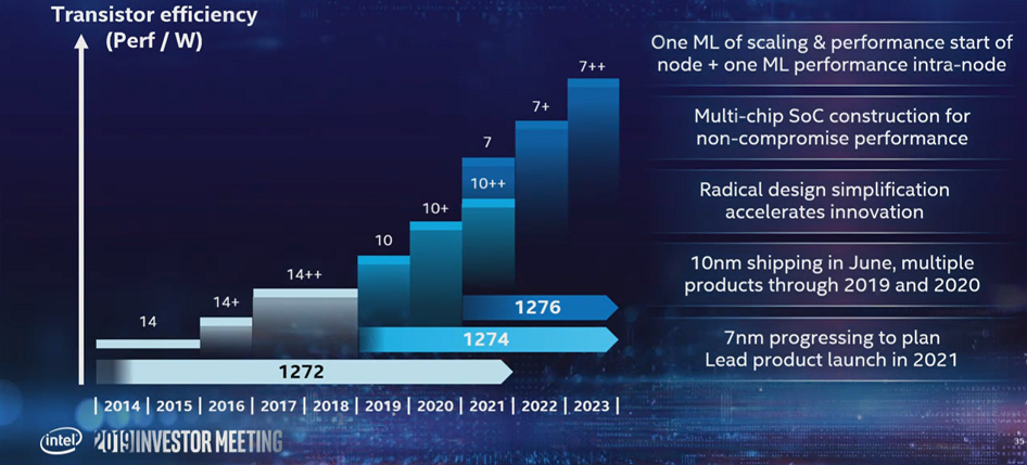
If you look at their plans for the 10 nanometer node, that works out to two cycles of Moore’s Law in three years, which is actually back to its original concept of doubling transistor density every 18 months. Whether than actually comes to pass remains to be seen.
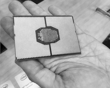
With Intel’s current schedule, the 7 nanometer node will debut in 2021, with a 7nm+ kicker in 2022, and a 7nm++ in 2023. That leaves just two years between the first 10 nanometer chips (which will ship next month in the form of the “Ice Lake” client processor) and the first 7 nanometer chips. The 7 nanometer products will also sync up with the Foveros and EMIB technologies and will be the first Intel manufacturing process to employ of extreme ultraviolet (EUV) lithography, which is set to drive transistor etching for future nodes as well.
The first 7 nanometer chip out of the chute will be Intel’s upcoming Xe GPU, which is being aimed at the AI and HPC markets and which we first detailed here. For the investor crowd that doesn’t follow the HPC market closely, Renduchintal reminded them that Xe will power Aurora, the first exascale supercomputer to be installed in the United States in 2021. The new GPU will also use the Foveros technology, although it’s not clear what that actually entails. (It wouldn’t surprise us if a bunch of Xeon cores ended up in the GPU package.)
That fact that Intel is leading its 7 nanometer charge with its first discrete GPU is indicative of the competitive landscape of the HPC/AI accelerator space. Not only has Nvidia captured much of that market already, but with AMD chalking up a big GPU (and CPU) win with the Department of Energy’s Frontier exascale system, Intel has to account for a battle on two fronts.
Of course, we’re getting a little ahead of ourselves, since Intel’s 10 nanometer story has yet to play out. Fortunately, Navin Shenoy, general manager of the Data Center Group, was on hand to offer some guidance in this regard. According to Shenoy, Intel’s first 10 nanometer processor for the datacenter, “Ice Lake SP,” is already sampling to some customers and is slated to start shipping in the first half of 2020. That will be followed by the next-generation Xeon, codenamed “Sapphire Rapids,” in 2021. Give that timeframe, its looks like this will be CPU that will end up in Aurora, alongside the aforementioned Xe GPUs.
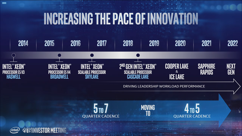
If all of this sounds fast-paced, Shenoy also let it be known that starting now, the cadence of processor rollouts will be increased from the current five to seven quarters to four to five quarters. Which means Intel will be cranking out new chips in a given product line essentially every year, whether there’s a new process node to land on or not. The rationale for all this rapid-fire chipmaking is that the total addressable datacenter market is growing so fast – Intel pegs it at $223 billion by 2023 – there will be opportunities aplenty for new silicon.
“In a world where there is near insatiable appetite for computing, and in a world where computers are in every increasing demand, we are going to pick up the pace,” said Shenoy.