


We have been talking about silicon photonics so long that we are, probably like many of you, frustrated that it already is not ubiquitous. But the good news is that advances in electrical signaling, after hitting a wall a decade ago when the talk of practical silicon photonics interconnects first really got going, continued to evolve and we have not really had to resort to silicon photonics yet.
With electrical interconnects between components being far less expensive, this has been a boon for the price numerator part of the price/performance equation, even though silicon photonics has an advantage in the denominator performance part of that equation. Over time, electrical signaling is getting shorter and shorter as the bandwidth goes up, and it is getting noisier and noisier, too. The day will inevitably come where we will shift from electrons to photons as electromagnetic signaling method and from copper to fiber optic glass as signaling media.
This curve, from a presentation that Nvidia chief scientist Bill Dally gave at the Optical Fiber Communication conference way back in March, makes the case pretty well:
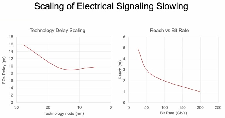
There is no arguing with those curves, although you can bend them a bit with materials science wizardry.
Nvidia signed a research and development partnership with Ayar Labs several weeks ago, and we sat down and had a chat with Charlie Wuischpard, chief executive officer at the silicon photonics startup, to talk about what the two would be working on. Nvidia has participated in the Series C fundraising that Ayar Labs did earlier this year, when it raked in $130 million to develop its out of band lasers and silicon photonics interconnects. Hewlett Packard Enterprise, which also inked a deal in February of this year with Ayar Labs to figure out how to bring silicon photonics to the Slingshot interconnect, was also an investor in that funding round from April of this year. Ayar Labs had early backing from Intel as well, even though Intel wants to embed lasers inside of chips instead of pumping in laser signals from outside of chips as Ayar Labs is doing. (If there is anything that is true right now, it is that Intel cannot afford to do anything wrong right now. So it is good that Intel is hedging its bets with silicon photonics.)
At that time of the April funding, we talked to Wuischpard at length about where silicon photonics fits into modern systems – and where it doesn’t yet fit, and more recently, we got some hints about what might develop specifically at Nvidia.
We subsequently became aware of the presentation mentioned above that Dally gave at OFC 2022, which very specifically outlines the goals of co-packaged optics using dense wave division multiplexing, or DWDM, and how silicon photonics might be used as a transport to cross connect racks and racks of GPU compute engines.
This presentation shows an unnamed concept machine, like the “Echelon” concept exascale system that Dally’s team developed way back in 2010 and that we caught wind of in 2012. That machine had special math engines – not GPUs – with high radix electrical switching between them and Cray “Aries” optical interconnects between racks of machines. And that Echelon machine was obviously never commercialized, and Nvidia instead took the NVSwitch memory interconnect that Dally was working on at Nvidia Research and pulled it into production way early to make what are in essence big iron NUMA GPU processor complexes interlinked by fat, multiport InfiniBand pipes instead.
With the initial DGX systems based on the NVSwitch, Nvidia could only scale to sixteen GPUs in a single image with the “Volta” V100 GPU accelerators, and with the “Ampere” A100 GPU accelerators, which had a lot more oomph, Nvidia had to double the bandwidth to each GPU and therefore had to cut the radix of NVSwitch by a factor of two, and therefore could only gang up eight GPUs into a single image. With the leaf/spine network of NVSwitches that was announced earlier this year with the “Hopper” H100 GPU accelerators, which will ship later this year, Nvidia can gang up 256 GPUs into a single memory fabric, which is a huge factor of improvement.
But in the end, the NVSwitch fabric at the heart of the DGX H100 SuperPOD is still essentially a way to create a scale-up NUMA machine, and it is absolutely limited by electrical cabling. And the scale of NVSwitch, even with the Hopper generation, does not even come close to the tens of thousands of GPUs that the hyperscalers have lashed together to run their largest AI workloads.
“I can’t go into a lot of details,” Wuischpard tells The Next Platform with a laugh. [Like, no kidding, man.] “You know, we are a physical layer solution, and there’s so much that sits above that in terms of the software and the orchestration between the GPUs, their memory, and the CPUs. We are not involved in any of that stuff. So I guess you can think of us as a physical enablement for the future. And it is a multi-phased approach that goes somewhere. This is not just a tire kicking exercise. But we have to prove ourselves, within some of the parameters and we have to hit some milestones.”
We hope that clears that up. . . . [Our turn to laugh.]
In any event, let’s now turn to the presentation that Dally gave at OFC 2022, which jumps ahead to what some future GPU accelerated system might look like with silicon photonics interconnects.
Before we get into that, let’s just look at the limitations on bandwidth and power between the GPUs or switches, the printed circuit boards they attach to, and the cabinets they might be pooled in, which sets the stage for silicon photonics interconnects:

The rule is simple. The shorter the links, the higher the bandwidth and the lower the energy consumed to shift a bit. And this table below lays out the relative power, cost, density and each of interposer, printed circuit board, co-packaged optics, electrical cables, and active optical cables, all of which are wires that comprise different levels of a modern system. Have a gander at this:
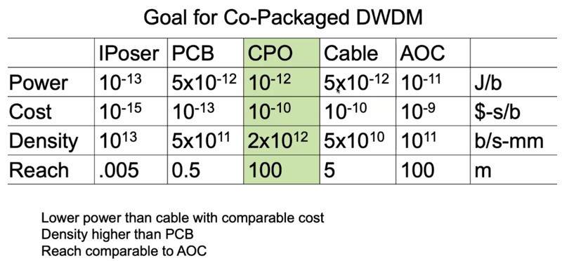
The goal for co-packaged optics using DWDM is to have lower power consumption than an electrical cable but with a similar cost, have a reach comparable to an active electrical cable, and offer signal density that is on par with a printed circuit board.
Here’s Dally’s sketch of what that DWDM signaling might look like:

And here is the block diagram of how the GPU and the NVSwitch would have optical engines to convert electrical signaling to optical signaling to create an NVSwitch network of the GPUs:
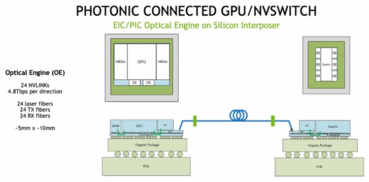
There are 24 fibers coming off each Optical Engine, and they initially would run at 200 Gb/sec signaling rates, for a combined 4.8 Tb/sec of bandwidth. Each GPU has a pair of these to give it bi-directional bandwidth into and out of an NVSwitch fabric. An NVSwitch with six optical engines would therefore be rated at 28.8 Tb/sec raw and 25.6 Tb/sec after encoding overhead is taken off.
Here is how the energy consumption works out across the various barriers between device components in the Nvidia silicon photonics concept machine:
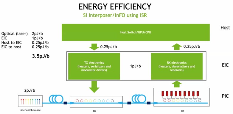
The 3.5 picojoules per bit to move data in and out between the GPU and the switch is right on par with the goals that Dally set out in the table above. We suspect that the costs still have to come down to make co-packaged optics acceptable for compute engines, but a lot of work is being done here and everyone is extremely motivated
The electrical signaling used on the embedded NVSwitch fabric on the current DGX-A100 systems has a range of about 300 centimeters and moves data at 8 picojoules per bit. The goal is silicon photonics to do it at half the energy and boost the range to as far as 100 meters between devices.
When that happens, you can disaggregate GPUs and switches in the architecture – and while Nvidia’s concept machine doesn’t show this, the CPUs can have optical engines, too, and they can be disaggregated, too.
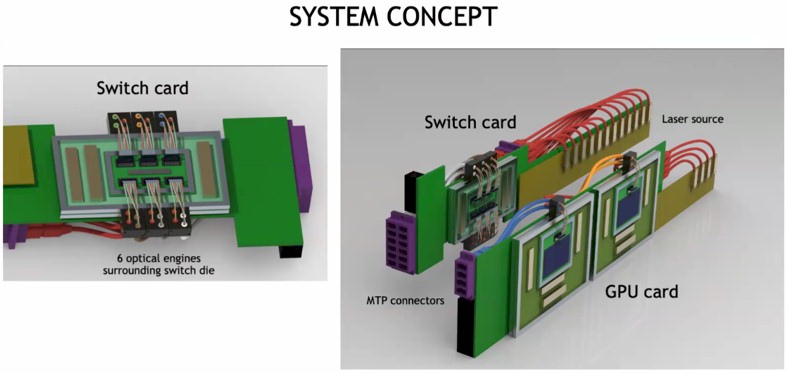
Here is what the GPU and switches with co-packaged optics might look like:
And here is how GPUs and NVSwitches with CPO links might be aggregated:
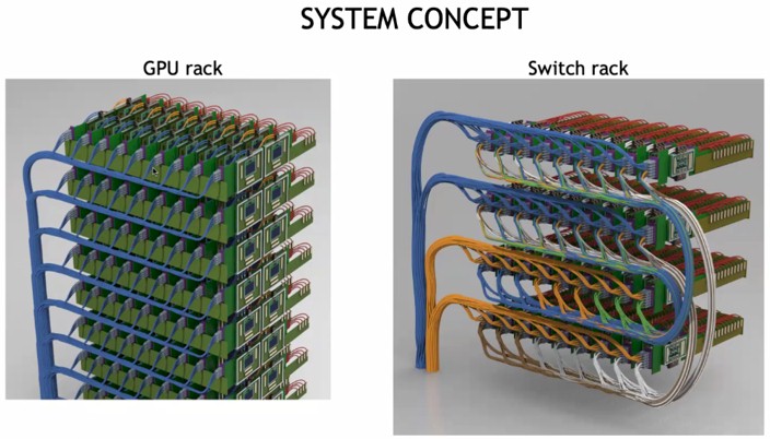
The external laser sources take up a lot of space, but this also means racks can be a lot less dense because connections between devices can be longer. This will make cooling easier, and the lasers out to be replaceable, too. If all of this stuff runs cooler, the lasers will work better as well. Density is overrated, and in many cases, as with the DGX systems for instance, the machines end up being so hot that you can only half-populate the racks anyway because the power density and cooling needs are more than most datacenters can handle.
You will note that the rows of GPUs and switches above are oriented vertically, which aids in cooling. And they are not mounted on giant printed circuit boards with sockets, either, which will help lower overall system costs to help pay for the use of optical interconnects.