


The in-person GPU Technical Conference held annually in San Jose may have been canceled in March thanks to the coronavirus pandemic, but behind the scenes Nvidia kept on pace with the rollout of its much-awaited “Ampere” GA100 GPU, which is finally being unveiled today. All of the feeds and speeds and architectural twists and tweaks have not yet been divulged, but we will tell you what we know and do a deep architecture dive next week when that data is available.
Here is the most important bit, right off the bat. The Ampere chip is the successor not only to the “Volta” GV100 GPU that was used in the Tesla V100 accelerator announced in May 2017 (aimed at both HPC and machine learning training workloads) but, as it turns out, the chip is also the successor to the “Turing” TU102 GPU used in the Tesla T4 accelerator launched in September 2018 (aimed at graphics and machine learning inference workloads). That’s right. Nvidia has created a single GPU that can not only run HPC simulation and modeling workloads considerably faster than Volta, but also converges the new-fangled machine learning inference based on Tensor Cores onto one device. But wait, that’s not all you get. With the Ampere chip, Nvidia has also announced that it has been working with the Spark community to accelerate that in-memory, data analytics platform with GPUs for the past several years, and it is now also ready. And thus, now the massive amount of preprocessing as well as the machine learning training and the machine learning inference can now be done all on the same accelerated platforms.
There are still CPUs in these systems, but they are relegated to handling serial processes in the code and managing large blocks of main memory. The bulk of the computing in this AI workflow is being done by the GPUs, and we will show the dramatic impact of this in a separate story detailing the new Nvidia DGX, HGX, and EGX systems based on the Ampere chips after we go through the technical details we have gathered about the new Ampere GPUs.
Let’s start with what we know about the Ampere GA100 GPU. The chip is etched in the 7 nanometer processes of Taiwan Semiconductor Manufacturing Corp, and the device weighs in at 54.2 billion transistors and comes in at a reticle-stretching 826 square millimeters of area.
The “Pascal” GP100 GPU announced in April 2016 was etched with 16 nanometer processes by TSMC, weighed in at 15.3 billion transistors, and had an area of 610 square millimeters. This was a ground-breaking chip at the time, and it seems to lack heft by comparison. The Volta GP100 from three years ago, etched in 12 nanometer processes, was almost as large at 815 square millimeters with 21.1 billion transistors. Ampere has 2.6X as many transistors packed into an area that is 1.4 percent bigger, and what we all want to know is how those transistors were arranged to yield a massive boost in performance.
Figuring out the double precision floating point performance boost moving from Volta to Ampere is easy enough. Paresh Kharya, director of product management for datacenter and cloud platforms, said in a prebriefing ahead of the keynote address by Nvidia co-founder and chief executive officer Jensen Huang announcing Ampere that peak FP64 performance for Ampere was 19.5 teraflops (using Tensor Cores), 2.5X larger than for Volta. So you might be thinking that the FP64 unit counts scaled with the increase of the transistor density, more or less. But actually, the performance of the raw FP64 units in the Ampere GPU only hits 9.7 teraflops, half the amount running through the Tensor Cores (which did not support 64-bit processing in Volta.)
We will be doing a detailed architectural dive, of course, but in the meantime, here are the basic feeds and speeds of the device, and it is just absolutely jammed packed with all kinds of compute engines in its 108 streaming multiprocessors (also known as SXMs):
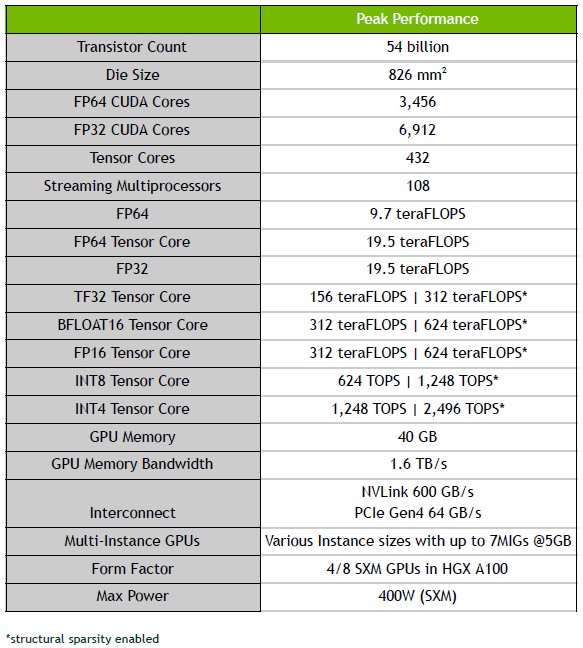
On single precision floating point (FP32) machine learning training and eight-bit integer (INT8) machine learning inference, the performance jump from Volta to Ampere is an astounding 20X. The FP32 engines on the Ampere GV100 GPU weigh in at a total of 312 teraflops and the integer engines weigh in at 1,248 teraops. Obviously, 20X is a very big leap – the kind that comes from clever architecture, like the addition of Tensor Cores did for Volta.
One of the clever bits in the Ampere architecture this time around is a new numerical format that is called Tensor Float32, which is a hybrid between single precision FP32 and half precision FP16 and that is distinct from the Bfloat16 format that Google has created for its Tensor Processor Unit (TPU) and that many CPU vendors are adding to their math units because of the advantages it offers in boosting AI throughput. Every floating point number starts with a sign for negative or positive and then has a certain number of bits that signify the exponent, which gives the format its dynamic range, and then another set of bits that are the signifcand or mantissa, which gives the format its precision. Here is how Nvidia stacked them up when talking about Ampere:

The IEEE FP64 format is not shown, but it has an 11-bit exponent plus a 52-bit mantissa and it has a range of ~2.2e-308 to ~1.8e308. The IEEE FP32 single precision format has an 8-bit exponent plus a 23-but mantissa and it has a smaller range of ~1e-38 to ~3e38. The half precision FP16 format has a 5-bit exponent and a 10-bit mantissa with a range of ~5.96e-8 to 65,504. Obviously that truncated range at the high end of FP16 means you have to be careful how you use it. Google’s Bfloat16 has an 8-bit exponent, so it has the same range as FP32, but it has a shorter 7-bit mantissa, so it has less precision than FP16. With The Tensor Float32 format, Nvidia did something that looks obvious in hindsight: It took the exponent of FP32 at eight bits, so it has the same range as either FP32 or Bfloat16, and then it added 10 bits for the mantissa, which gives it the same precision as FP16 instead of less as Bfloat16 has. The new Tensor Cores supporting this format can input data in FP32 format and accumulate in FP32 format, and they will speed up machine learning training without any change in coding, according to Kharya. Incidentally, the Ampere GPUs will support the Bfloat16 format as well as FP64, FP32, FP16, INT4, and INT8 – the latter two being popular for inference workloads, of course.
Another big architectural change with the Ampere GPU is that the Tensor Cores have been optimized to deal with the sparse matrix math that is common in AI and some HPC workloads and not the dense matrix math that the prior Volta and Turing generations of Tensor Cores employed. This spare tensor ops acceleration is available with Tensor Float 32 (TF32), Bfloat16, FP16, INT4, and INT8 formats, and Kharya says that this feature speeds up sparse matrix math execution by a factor of 2X. We are not sure where all of the 20X speedup cited for single-precision and integer performance comes from, but these are part of it.
Another big change with the Ampere GA100 GPU is that it is really seven different baby GPUs, each with their own memory controllers and caches and such, and these can be ganged up to look like a big winking AI training chip or a collection of smaller inference chips without running into memory and cache bottlenecks like the Volta chips had when trying to do inference work well. This is called the Multi Instance GPU, or MIG, part of the architecture.
The Chip Is Not By Itself The Accelerator
The Ampere GA100 GPU is, of course, part of the Tesla A100 GPU accelerator, which is shown below:
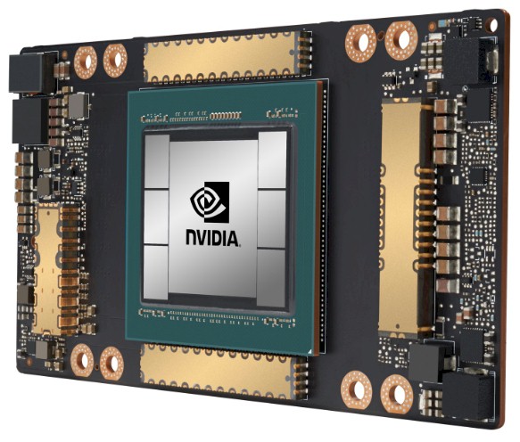
The Tesla A100 GPU accelerator looks like it plugs into the same SXM2 slot as the Volta V100 GPU did, but there are no doubt some changes. The Ampere package comes with six banks of HBM2 memory, presumably with four stacks, with 40 GB of memory capacity. That is 2.5X more memory than the initial Volta V100 accelerator cards that came out three years ago, and 25 percent more HBM2 memory than the 32 GB that the enhanced V100s eventually got. While the memory increase is modest, the memory bandwidth boost is perhaps more important, rising to 1.6 TB/sec across the six HBM2 banks on the Tesla A100 package, up 78 percent from the 900 GB/sec of the Tesla V100. So many workloads in HPC and AI are memory bandwidth constrained, and considering that a CPU is lucky to get more than 100 GB/sec of bandwidth per socket, this Tesla A100 accelerator is a bandwidth beast, indeed.
The 40 GB HBM2 capacity across six banks are both weird numbers, just like the number of MIGs, at 7 per GA100 chip, is also weird. We would have expected eight MIGs and 48 GB of capacity because we believe in multiples of 2, so maybe there is some yield improvement by ignoring some dud portions on the GA100 chip and the other components in the Tesla A100 package. That’s what we would do if we were Nvidia. That also means, if we are right, there are more than 108 SXMs on the chip – 128 is a good base 2 number – and probably eight MIGs, each with 16 SXMs on them. The point is – again if we are right – that means there is another 15 percent or so of compute capacity and another 20 percent of memory capacity possibly inherent in the Tesla A100 device, which can be productized as yields improve at TSMC.
The Tesla A100 accelerator is going to support the new PCI-Express 4.0 peripheral slot, which has twice the bandwidth as the PCI-Express 3.0 interface used in the Tesla V100 variants based on PCI-Express, as well as the NVLink 3.0 interconnect, which runs at 600 GB/sec across what we presume are six NVLink 3.0 ports that come off the Ampere GPU. That’s twice the bandwidth per GPU and into an NVSwitch interconnect ASIC, which Nvidia unveiled back in April 2018, and it looks like there is not an update to NVSwitch since the DGX and HGX servers that Nvidia has designed have only eight Ampere GPUs compared to sixteen GPUs with the Volta generation.
Next up, we will talk about the systems using the new Ampere GPU and what kind of performance and value they will bring to the datacenter.