


The memory market can be a volatile one, swinging from tight availability and high prices one year to plenty of inventory and falling prices a couple of years later. The fortunes of vendors can similarly swing with the market changes, with Samsung recently displacing Intel at the top of the semiconductor space as a shortage in the market drove up prices and, with it, the company’s revenues.
High performance and high-speed memory is only going to grow in demand in the HPC and supercomputing arena with the rise of technologies like artificial intelligence (AI), machine learning and graphics processing, and getting a growing amount of focus in the industry is High-Bandwidth Memory-2 (HBM2). There also is demand for GDDR5 and plans by many vendors to soon start rolling out GDDR6. There are tradeoffs – HBM2 is more expensive but enables lowers power consumption. All that said, Samsung, Intel, Advanced Micro Devices, Nvidia, NEC and others all are coming out products with HBM2.
As we’ve noted at The Next Platform, Intel is getting ready to finally bring “Lake Crest” deep learning chip – which will include 32 GB of 3D stacked HBM2 – that is based on the architecture the company inherited almost two years ago when it acquired Nervana Systems and will compete with Nvidia and its cadre of deep learning GPUs and appliances. The Lake Crest chip is the beginning of an aggressive roadmap Intel is laying out for the Nervana technology, which includes what will be the follow-up to Lake Crest, called “Knights Crest.” Intel also has integrated HBM2 in its Stratix 10 MX field-programmable gate array (FPGA), with the ability to put up to two HBM2 devices into a single package for a maximum memory bandwidth of up to 512 GB/s.
Nvidia is leveraging HBM2 in a range of products, including its powerful Titan V PC GPU, which includes 12GB of HBM2, and Tesla “Volta” V100 datacenter GPU aimed at such HPC workloads as AI training and inference and high-end graphics. The Tesla V100 includes 16 GB of HBM2. Nvidia also has used HBM2 in other products, such as Quadro GPUs based on the “Pascal” architecture. AMD is arming its new “Vega” Radeon GPUs with HBM2, and at the recent CES 2018 show, both AMD and Intel rolled out chips that include the Vega Radeon GPUs. At the same time, AMD is said to be planning to use GDDR6 in future products.
Fujitsu is building out its Post-K supercomputer – its upcoming follow-up to the powerful K system – and is moving away from the Sparc64 chips that power the current system and instead opting instead for an ARM-based processor design. The system will be able to run the same machine learning training and inference tasks that other systems now are doing using Intel Xeon processors paired with Nvidia GPUs. But as we laid out last year, Fujitsu also is building its own deep learning processor, or DLU, for pure deep learning workloads and which is being built by company engineers from the ground up. Part of the DLU’s makeup will be HBM2 memory. For its part, NEC is building its “Aurora” Vector Engine processor for its upcoming “Tsubasa” system. Aurora will include up to 48 GB of HBM2 memory – or four times that in Nvidia’s Tesla V100 GPU accelerator – with each cache segment having three HBM2 interfaces that are linked to HBM2 main memory that is stacked eight dies high.
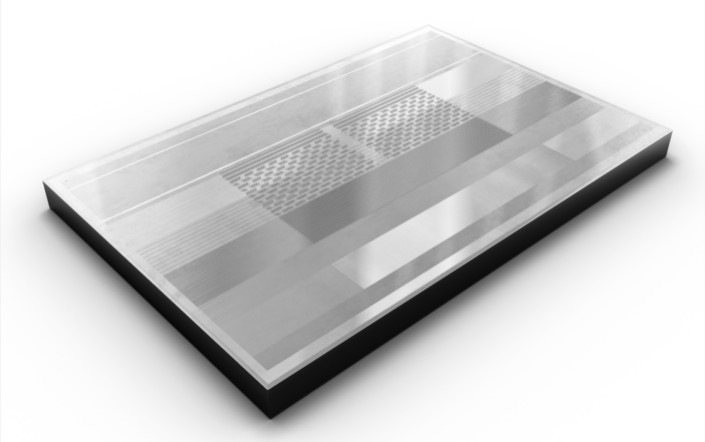
Samsung is now pressing its advantage in the memory market. The company this month announced it has begun mass production of its next-generation 8 GB HBM2, dubbed “Aquabolt.” The company is claiming that the new memory chip will offer 2.4 Gb/sec data transfer speed per pin, the fastest on the market and the next step in accelerating the use to AI and supercomputing. The high-speed data transfer rate at 1.2V means a 50 percent performance boost per package over Samsung’s previous “Flarebolt” devices, which offers 1.6 Gb/sec at 1.2V and 2 Gb/s at 1.35V. The Aquabolt offers faster speeds without an accompanying increase in power.
According to Samsung, a single 8 GB HBM2 package will deliver 307 GB/sec data bandwidth, or 9.6 times faster transmission than an 8 Gb GDDR4 chip. With four Aquabolt packages, a system will have 1.2 TB/sec bandwidth.
To get this performance, Samsung engineers developed technologies aimed at TSV (Through Silicon Via) design and thermal control. An 8 GB package includes eight 8 GB HBM2 dies that are interconnected via more than 5,000 TSVs per die. At the same time, strong thermal control in each package was accomplished by increasing the number of thermal bumps between each of the dies. Thermoelectric cooling occurs at each bump, so adding more helped Samsung engineers provide better thermal control capabilities to Aquabolt.
The fluctuating memory market will continue to see rapid changes and evolution. Samsung is using its size to put pressure on other players in the space, which is already starting to see some fallout, with Toshiba – the second largest provider of NAND memory chips – selling its memory business to a consortium led by venture capital firm Bain for $18 billion, bypassing offers from Western Digital. There also will be the continued development of new technologies, including HBM3 and GDDR6.