The memory market can be a volatile one, swinging from tight availability and high prices one year to plenty of inventory and falling prices a couple of years later. The fortunes of vendors can similarly swing with the market changes, with Samsung recently displacing Intel at the top of the semiconductor space as a shortage in the market drove up prices and, with it, the company’s revenues.
High performance and high-speed memory is only going to grow in demand in the HPC and supercomputing arena with the rise of technologies like artificial intelligence (AI), machine learning and graphics processing, and getting a growing amount of focus in the industry is High-Bandwidth Memory-2 (HBM2). There also is demand for GDDR5 and plans by many vendors to soon start rolling out GDDR6. There are tradeoffs – HBM2 is more expensive but enables lowers power consumption. All that said, Samsung, Intel, Advanced Micro Devices, Nvidia, NEC and others all are coming out products with HBM2.
As we’ve noted at The Next Platform, Intel is getting ready to finally bring “Lake Crest” deep learning chip – which will include 32 GB of 3D stacked HBM2 – that is based on the architecture the company inherited almost two years ago when it acquired Nervana Systems and will compete with Nvidia and its cadre of deep learning GPUs and appliances. The Lake Crest chip is the beginning of an aggressive roadmap Intel is laying out for the Nervana technology, which includes what will be the follow-up to Lake Crest, called “Knights Crest.” Intel also has integrated HBM2 in its Stratix 10 MX field-programmable gate array (FPGA), with the ability to put up to two HBM2 devices into a single package for a maximum memory bandwidth of up to 512 GB/s.
Nvidia is leveraging HBM2 in a range of products, including its powerful Titan V PC GPU, which includes 12GB of HBM2, and Tesla “Volta” V100 datacenter GPU aimed at such HPC workloads as AI training and inference and high-end graphics. The Tesla V100 includes 16 GB of HBM2. Nvidia also has used HBM2 in other products, such as Quadro GPUs based on the “Pascal” architecture. AMD is arming its new “Vega” Radeon GPUs with HBM2, and at the recent CES 2018 show, both AMD and Intel rolled out chips that include the Vega Radeon GPUs. At the same time, AMD is said to be planning to use GDDR6 in future products.
Fujitsu is building out its Post-K supercomputer – its upcoming follow-up to the powerful K system – and is moving away from the Sparc64 chips that power the current system and instead opting instead for an ARM-based processor design. The system will be able to run the same machine learning training and inference tasks that other systems now are doing using Intel Xeon processors paired with Nvidia GPUs. But as we laid out last year, Fujitsu also is building its own deep learning processor, or DLU, for pure deep learning workloads and which is being built by company engineers from the ground up. Part of the DLU’s makeup will be HBM2 memory. For its part, NEC is building its “Aurora” Vector Engine processor for its upcoming “Tsubasa” system. Aurora will include up to 48 GB of HBM2 memory – or four times that in Nvidia’s Tesla V100 GPU accelerator – with each cache segment having three HBM2 interfaces that are linked to HBM2 main memory that is stacked eight dies high.
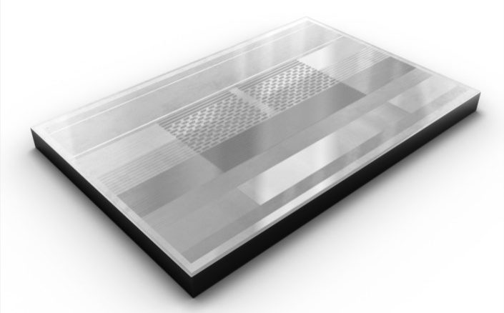
Samsung is now pressing its advantage in the memory market. The company this month announced it has begun mass production of its next-generation 8 GB HBM2, dubbed “Aquabolt.” The company is claiming that the new memory chip will offer 2.4 Gb/sec data transfer speed per pin, the fastest on the market and the next step in accelerating the use to AI and supercomputing. The high-speed data transfer rate at 1.2V means a 50 percent performance boost per package over Samsung’s previous “Flarebolt” devices, which offers 1.6 Gb/sec at 1.2V and 2 Gb/s at 1.35V. The Aquabolt offers faster speeds without an accompanying increase in power.
According to Samsung, a single 8 GB HBM2 package will deliver 307 GB/sec data bandwidth, or 9.6 times faster transmission than an 8 Gb GDDR4 chip. With four Aquabolt packages, a system will have 1.2 TB/sec bandwidth.
To get this performance, Samsung engineers developed technologies aimed at TSV (Through Silicon Via) design and thermal control. An 8 GB package includes eight 8 GB HBM2 dies that are interconnected via more than 5,000 TSVs per die. At the same time, strong thermal control in each package was accomplished by increasing the number of thermal bumps between each of the dies. Thermoelectric cooling occurs at each bump, so adding more helped Samsung engineers provide better thermal control capabilities to Aquabolt.
The fluctuating memory market will continue to see rapid changes and evolution. Samsung is using its size to put pressure on other players in the space, which is already starting to see some fallout, with Toshiba – the second largest provider of NAND memory chips – selling its memory business to a consortium led by venture capital firm Bain for $18 billion, bypassing offers from Western Digital. There also will be the continued development of new technologies, including HBM3 and GDDR6.


Samsung has the lead while SK Hynix is behind for HBM2 and I can not think of any other HBM2 makers. HBM2’s cost will remain high without much in the way of competition with Samsung that major supplier. Samsung will have no problems amortizing its HBM2/Next HBM product’s R&D and plant costs so even if there is some competition in the future Samsung can more than likely lower its prices without suffering much in the way of compared to any new HBM2 competition from any newer HBM2 makers, as startup/R&D costs for HBM2 production are relatively high. I think that Samsung will be the major HBM2 innovator in the market place for the foreseeable future with SK Hynix hopefully being able to ramp up its HBM2 production also.
Samsung’s Aquabolt HBM2 will do wonders for those Mashup on an EMIB/MCM Intel/AMD SOC/Discrete GPU/HBM2(Single HBM2 Stack) based SKUs that can use all the extra bandwidth that a single stack of HBM2 can provide. Let’s not forget that Vega’s HBCC/HBC(HBM2) IP can treat any HBM2 like a L4 GPU cache and use that HBM2/L4 HBC(High Bandwidth Cache) to leverage a larger pool of Virtual VRAM paged out to regular system DIMM based DRAM or even SSD based virtual VRAM paged to NVM/SSD/Hard Drive. So the more the bandwidth to that single stack of HBM2/Cache can offer the better for performance as the GPU will mostly feed from the HBM2 and all the paging to and from slower Virtual VRAM can happen in the background via the HBCC(High Bandwidth Cache Controller) IP.
Maybe Samsung/Other HBM2 makers and JEDEC can focus on maybe some HBM2 single stack options with even higher bandwidth as those single stacks of HBM2 for Vega based graphics will be able to make use of that Vega HBCC/HBC(HBM2) IP using lower cost 4GB HBM2 stacks with a larger amount of virtual VRAM paged to and from HBC(HBM2) to secondary RAM/SSD. So laptops using any Intel/AMD SOC/semi-custom AMD discrete Vega GPU on the EMIB/MCM will do well for Blender 3d/Maya/other graphics software where virtual VRAM can be as large as needed and not limited to only the capacity of the HBM2. Maybe even an HBM-2.5 JEDEC standard where the HBM stack can be made a little larger and the interface could be bumped up from 1024 to 1536 bits wide, or they can just go with higher burst clock rates for some usage where extra HBM2 bandwidth is required.
AMD did show off a discrete mobile Vega variant at CES with a single stack of HBM2(4GB) so maybe there will be more laptop options in the next few months for those graphics design/pro graphics folks to look forward to with AMD’s Vega graphics and the HBCC/HBC IP that actually is the more interesting part of the Vega GPU design than any gaming only focused designs from Nvidia. I’d rather pay more to get any Intel/AMD(Vega) EMIB or even a discrete mobile AMD Vega GPU SKU in a laptop form factor make use of HBM2 simply because of that HBCC IP in Vega that has the ability to treat any amount of HBM2 as a HBC so Blender 3D/other 3d graphics(Non Gaming) workloads do not run out of VRAM for lack of physical VRAM capacity for the GPU.
Nvidia appears to be only using HBM2 currently for its professional compute/AI market products with Nvidia’s consumer GPU SKUs making use of GDDR5/5X and most likely GDDR6 in 2018. Considering how much the coin miners have driven up the price of GPUs lately it probably would be better for the makers to switch to HBM2 as soon as possible and pass that extra wholesale cost onto the retail market as current demand for GPUs with any form of memory is being driven high anyways mostly by demand. So Samsung and SK Hynix should be investing more in increasing HBM2 production because the more the GPU/Compute industry makes use of HBM2 the faster the fixed costs will come down as HBM2 plants and equipment costs become fully amortized sooner via higher volumes of HBM2 unit sales. GPUs are in such demand lately that HBM2’s cost relative to the GPUs overall cost at retail is actually going down even with HBM2 costing much more than GDDR5/5X/6, such has that coin mining demand so affected GPU demand pricing at the retail level regardless of GPU VRAM used.
The uncertainty of the crypto demand for GPUs is the whole reason that demand is currently outstripping supply. In order to keep up with current demand, output would have had to be increased perhaps 2 months ago, but 2 months ago it was not known that strong demand from crypto miners would now exist. A decision to put HBM into all GPUs must be made much further in advance of product availability than 2 months. Perhaps more like a year+? If GPU makers have decided they cannot rely on the crypto market enough to justify increasing supply then they surely can’t rely on it enough to justify making costly architectural decisions a year or more in advance that would have far-reaching effects for their competitiveness in the market. It’s unreasonable to expect the crypto market to result in a constant state of demand outstripping supply. At some point demand will likely catch up, and it is entirely possible to end up with a glut of cards in the channel if mining demand suddenly collapses. Imagine ending up with a glut of expensive to make HBM2 cards while your competitor has cheaper to produce GDDR6 cards. A competitor with cheaper GDDR6 cards might even be able to have more confidence in greater production knowing that if there is a sudden downturn in demand they will be in better shape than their competitors to get through the difficulty.
It’s the shader cores that the miners want and that’s not a function of the cost of the VRAM that a function of the number of GPU shader cores and the hashes/watt and the ability of those shader cores to hash at the optimal hashes/Watt metric.
The GPU VRAM costs are minimal compared to the Total Demand Market pricing that sets the cost of any product when demand outstrips supply. Companies like AMD where burned in the last round by the crypto mining market damand uncertainty and are justified in keeping their GPU production lower. Also AMD is trying to get the HBM(Now HBM2) supply economy of scale to kick in so HBM2/Newer can rightly replace the more power hungry GDDR5/5X/6 memory for VRAM usage.
So now is the perfect time for AMD/Others that use HBM2 to start using HBM2 on more than just the flagship gaming and professional GPU SKUs, so that HBM2 economy of scale can take over sooner and rightfully supplant the power/space inefficent GDDR# memory once and forever for GPU VRAM usage.
GDDR6 is not going to make most GPU cheaper as the miners demand will keep most Mid/High range GPU prices higher regardless of the cost of VRAM.
If those poor little gamers can not afford to pay the markups then let them eat XBONE-X and PS4-Pro! But AMD, Nvidia are not in business for any continued loss leader types of sales to the gaming only GPU market as there is now the GPU compute market to consider and that professional GPU market actually pays the proper markups for the GPU makers to funnd the massive amounts of investments in costly R&D, tapeout, and other costs assoicated with GPU design and production.
Using GDDR6 for cost savings in not going to be pased on to the consumer if the GPU makers do not legally have control over the demand market pricing of their GPU products at the retail level. It’s is illegal for GPU makers to enforce any Retail Pricing and GPU makers can only set their wholesale pricing and the current cost of GPUs is set at the Retail level by the laws of supply and demand and the GPU makers are not going to risk getting left with a load of GPU inventory that they have to declare as a write-down if they can not move the product by tax accounting time.
AMD and Nvidia currently are not in as direct competition with each other because current GPU demand is outstripping GPU supply such that both AMD and Nvidia need to actually raise their wholesale prices and make more revenues rather than letting their retail channel partners reap all the rewards of the mining demand market pricing pressure. The Retail Channel Partners are profiting more than AMD and Nvidia from AMD’s and Nvidia’s hard work and billions of dollars in investment in GPUs.
Gamers need to be forced to pay for HBM2’s creation and economy of scale along with the GPU professional compute/AI markets and HBM2 is needed for its power saving and space savings intrensic value. AMD’s Vega GPU micro-arch with that HBCC/HBC IP can allow for HBM2 of any size to become a last level cache to a rather larger 512 Terabytes of total addressable Vurtual VRAM paged out to regular slower system DDR4 DRAM or even SSD/Hard-Drive paged Virtual VRAM so the sooner that HBM2 is offered with all Vega products by AMD the sooner that those SKUs can have virtual VRAM that is larger than and physical VRAM on Vega/Newer GPUs.
Raja Koduri’s one defining contribution to AMD’s RTG and Vega GPU micro-arch is that Vega HBCC/HBC IP that allows for the HBM2 to become a last level GPU cache to a much larger pool of Virtual VRAM paged oit to slower DDR4 Memory or even SSD/Hard-Drive. So GPUs are not limited to just the capacity of the physical VRAM and HBM2 is necessary for that Vega HBCC IP to have any HBC(High Bandwidth Cache) in the form of HBM2 to use as a GPU last level cache to leverage any Virtual VRAM paged out to and from slower memory or SSD/Disk.
The sooner that All AMD Vega GPUs get HBM2 the better for all graphics uses for gaming or non gaming graphics usage. All GPUs should be required to use HBM2 to save on energy consumption and any power hungry memory shoud be taxed to make it more expensive than HBM2.
I too am excited by HBCC.
Long story short, the new reality is using less, but better gpu cache, and extending it as discussed.
Its a good fit for amd to sell 2x 4GB vegaS rather than 1x 8GB vega. They profit from gpuS, not samsung ram.
“Let’s not forget that Vega’s HBCC/HBC(HBM2) IP can treat any HBM2 like a L4 GPU cache and use that HBM2/L4 HBC(High Bandwidth Cache) to leverage a larger pool of Virtual VRAM paged out to regular system DIMM based DRAM or even SSD based virtual VRAM paged to NVM/SSD/Hard Drive.
… the GPU will mostly feed from the HBM2 and all the paging to and from slower Virtual VRAM can happen in the background”
Well put, and in an apu, the superfast hbm2 cache could double as “L4” cache for the Fabric linked cpu.
Its mad. A CPU with gigabytes of cache much faster than the few MB of l3 cache now.
There are several classic ‘b or B’ errors in this report.
“According to Samsung, a single 8 GB HBM2 package will deliver 307 Gb/s data bandwidth, or 9.6 times faster transmission than an 8 Gb GDDR4 chip. With four Aquabolt packages, a system will have 1.2 Tb/s bandwidth.”
The 307 Gb/s should be 307 GB/s. (2.4 Gb/s/pin x 8 channels x 128 b/channel.) With four devices you would have 1.2 TB/s peak bandwidth.
Similarly the Stratix 10 MX peak DRAM bandwidth is 512 GB/s not 512 Gb/s.
Also note Xilinx XCVU3xP UltraScale+ FPGAs (e.g. XCVU37P) are also slated to launch with these HBM2 devices.
I think HBM2 will still take some time to get into mainstream graphics cards because of its high cost of production. Also this much bandwidth is impossible for all GPUs to utilize.
That AMD went out on a long limb committing to unproven hbm memory for vega, imo, indicates the particular extra appeal it has for on die use with AMD’s mobile APUs (low power, compact & thin – not just fast).
Nvidia had far less reason to risk hbm, but they did anyway in some cases, such is it’s appeal.
Stuff happens. I think amd management made a smart bet, but there were unforeseen problems.
Its not in evidence yet (the intel/vega hybrid is not an apu imo – its just a Vega mobile dgpu), but the intent is surely there to mount it on the Amd apu die.