


AMD has been absent from the X86 server market for so long that many of us have gotten into the habit of only speaking about the Xeon server space and how it relates to the relatively modest (in terms of market share, not in terms of architecture and capability) competition that Intel has faced in the past eight years.
Those days are over now that AMD has successfully got its first X86 server chip out the door with the launch of the “Naples” chip, the first in a line of processors that will carry the Epyc brand and, if all goes well, carry AMD back into the datacenter where it can reap some revenue and profits as companies look for alternatives – and we think lower cost alternatives – to what the world’s largest chip maker provides.
The Epyc chips have been a long time in the making, with five years of rethinking how to make a better core and a better system than it had done in the later generations of the Opteron processors that put AMD on the server processor map back in the early 2000s. The world has changed a lot since then, of course, but the two socket server still reigns supreme, and with the Epyc architecture AMD has hopes of shaking up the order of things and selling fully loaded one-socket Epyc systems head-to-head against the mainstream, mid-line Xeon E5 processors that are typically deployed in two-socket systems in the datacenters of the world today. It will also sell its two-socket machines against beefier Intel boxes, but forgo expanding its line to systems with four or more sockets using NUMA clustering as Intel does. AMD has been trickling out performance stats here and there, pitting the Epyc chips against Intel’s current “Broadwell” Xeon E5 processors, and it has also been banging the drum for hybrid setups that marry the Naples Epyc processors with its “Vega” Radeon Instinct GPU accelerator cards for running HPC and machine learning workloads.
It is an ambitious strategy, and it is not guaranteed to work, but it does fit the data of the market pretty cleverly and gives AMD a fighting chance to get a slice of the server pie once again. And once that happens, AMD can fund more research and development and try to take an even bigger chunk.
With the Epyc launch down in Austin, Texas, what we finally get is a look at the feeds and the speeds of the Naples processors as well as a sense of how these chips stack up against the current Broadwell Xeon competition. AMD is also unveiling some features tucked away in the processors, including some interesting encryption circuits on the memory controllers that lock down data in flight.
The First In A Family
The initial members of the first generation of Epyc processors are known as the Epyc 7000s, and the very naming suggests that there will eventually be other members of the family. But thus far, AMD has been mum about this. Having said that, we have been expecting a converged CPU-GPU chip with 16 cores and an advanced but trimmed down GPU, and this could still yet come to pass and be very interesting for workstations and certain classes of servers that need to provide hybrid compute but do so in a much smaller form factor and power budget – and at a much lower cost, too. But no one is talking about this chip, and what it might be any more. And as we have previously pointed out, AMD could create or acquire a chipset that allows it to gang up multiple two-socket nodes in a NUMA cluster to expanding the memory addressing (it has several designs of its own from years gone by to tap), but thus far the company has indicated that it is not interested in such scale up capability. Suffice it to say, there is room in the line for the Epyc 3000, Epyc 5000, and Epyc 9000 should AMD decide to move up and down the market.
For the moment, AMD is intent on turning on all of the features in the Epyc 7000s for all of its SKUs and using this openness to try to wrestle some share away from Intel, which demarcates its server chip SKUs by on many dimensions, including core count, frequency, memory addressability, memory speed, interconnect speed, threading, and a slew of other features. In the Epyc 7000 line, AMD obviously has different SKUs with different numbers of cores and different clock frequencies, which all processor chip makers need to do to make the fullest use of their manufacturing yields to drive revenues. But the covers are off on memory capacity and speed and I/O capacity and bandwidth.
Importantly, Dan Bounds, senior director of enterprise products, tells The Next Platform that the future “Rome” generation of Epyc 7000 processors will be socket compatible with the Naples sockets, which means that motherboard and system makers can re-use their systems with the future Rome chips that are anticipated in early 2018 according to the company’s roadmaps. While AMD is not making any promises about socket compatibility beyond that, it would probably be best for the company if that same socket was used for the “Milan” Epyc 7000 series expected sometime before 2020 (it looks like maybe late 2019 in the roadmaps). Bounds is not committing to any path, but did warn us not to jump to the conclusion that the Milan socket would be incompatible. AMD is keeping its options open, depending on how technologies change in the server racket and how its server partners would respond to such a change. The typical cadence is to keep a socket for two generations these days, but those making a commitment to Epyc may require more longevity, and that puts an engineering constraint on the future even as it makes the present more possible.
The Epyc 7000s are system-on-chip designs, which means they do not require an external chipset to operate in single-socket mode or two expand out to two-sockets with NUMA interconnects. All the necessary I/O for linking the sockets is on the chips, as are all of the controllers to link out to memory and peripherals. Conceptually, here is what the Epyc 7000 block diagram looks like:
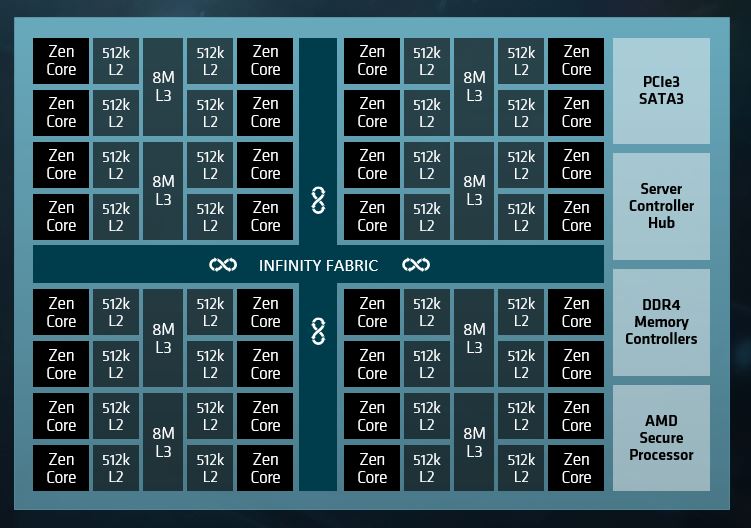
Do not take this diagram literally. The Epyc 7000 is actually comprised of eight separate processors that share a common socket and that are linked to each other through an on-package implementation of the Infinity fabric that is also used to scale out to a second socket, to main memory, to GPU accelerators, to flash storage, and to other PCI-Express 3.0 devices.
The computing elements on the Ryzen desktop and Epyc server chips are based on a four-core computing complex that looks like this:
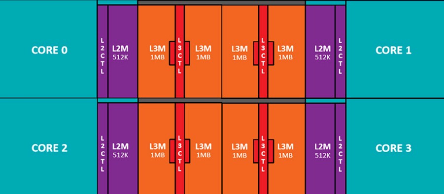
As you can see, the architecture uses a cores-out design, with the L3 memory controllers striped amongst the L3 cache and feeding into the L3 caches, which in turn are glued to the Zen cores by an L2 cache controller. The interconnect sits between all of these caches and cores and is used to link two four-core compute elements together; as far as we know, this is not the Infinity fabric as AMD talks about it. Each core has a 32 KB L1 cache and a dedicated 512 KB L2 cache, and there are eight slices of L3 cache that weigh in at 1 MB each that are segmented in 2 MB sections adjacent to each core but all cores can reach all caches (with varying latencies, of course). Two of these four-core compute elements are on a single chip, and there is no reason other than economics and yield that AMD did not just place all 32 cores on a single die. But placing eight cores on a die and then stitching them together using the Infinity fabric interconnect means that AMD can make a much cheaper 32-core socket than if it had did it as one 32-core monolith or even two 16-core segments.
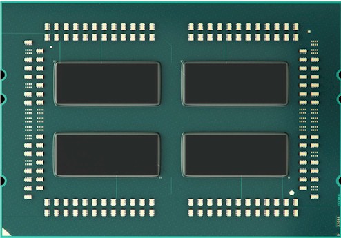
Here is what the back of the package showing the four dies looks like:
One of the issues that many of us are thinking about is what the latency and bandwidth is between those chiplets on the package, and how this may – or may not – impact performance. We don’t have any information about the latencies to move data across these segments of the Naples processor package, but AMD did supply us with some information about the bandwidth, as follows. Take a look:
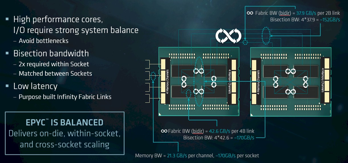
From this chart, we see that the bisectional bandwidth across the Infinity fabric links (there are four per chiplet) within the package is the same as the memory bandwidth for each Epyc 7000 socket. The NUMA interconnect running over half of the 128 PCI-Express 3.0 lanes when they are used to create a two-socket Epyc system provide the same 170 GB/sec of bandwidth. As the slide above suggests, AMD thinks there is plenty of bandwidth between the chiplets and across the sockets; what we want to know is what the relative latencies are between the chiplets on the die and across those two sockets. We would also like to get a sense what happens when the system is loaded up with lots of peripheral I/O – for instance, when the machine is loaded up with lots of GPU accelerators and flash memory – and also has a workload that has a lot of communication across those chiplets and sockets.
The new Secure Memory Encryption feature allows for memory to be partitioned and the segments to have their data encrypted in a way that does not impact application performance because the AES-256 cryptography is done in hardware, right on the memory controllers. This encryption is only available for memory that plus into the DIMM slots, which right now means DDR4 memory but in the future could mean NVDIMMs or 3D XPoint memory. Any encryption that is needed for flash or disk storage – data really at rest – has to be done with software-based encryption running on the CPU or offload accelerators added to the system. This SME feature, says Bounds, is aimed at securing all memory accesses, but is particularly useful for clients that are setting up multitenant systems where it is particularly bad for one user to see the data of another. This memory encryption works hand-in-glove with Secure Encrypted Virtualization, which encrypts the data stored on virtual machine instances on top of hypervisors. All of this functionality is transparent to the operating system and hypervisors and does not require any changes to applications. “This is the security that you can actually use,” says Bounds.
The Feeds And Speeds And Slots And Watts
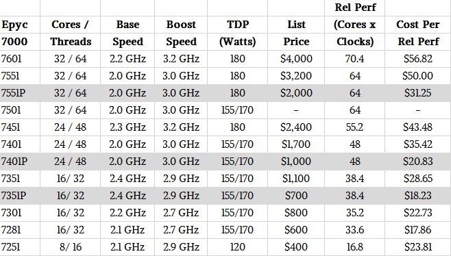
With the Epyc 7000s, all processors can be used in systems with either one or two sockets, but AMD has a few SKUs that are tuned up specifically to make the single socket a little extra juicy. Those chips designed with the extra bang for the buck for single-socket work have a P at the end of their names.
Each Epyc 7000 socket has eight memory channels, each with two DIMMs hanging off of it, and using 128 GB memory sticks (which no one does), the memory capacity can reach 2 TB per socket. With much less expensive 32 GB memory sticks, 512 GB is quite reasonable, and this is a very good amount of memory per socket. The Epyc 7000s can run with either 2.4 GHz or 2.67 GHz main memory, and in certain models, using the faster memory results in a 170 watt TDP instead of the 155 watt TDP. Clearly, the memory controllers have to work harder in some models to run faster and it is generating more heat.
Here is how the Epyc 7000s stack up against each other:
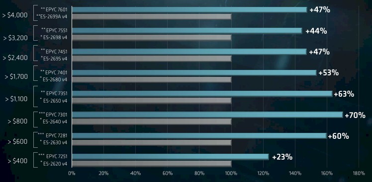
AMD has stacked up the Epyc 7000s against the current Broadwell Xeons, and at a given price point, it thinks it can deliver somewhere between 45 percent and 60 percent better bang for around the same bucks.
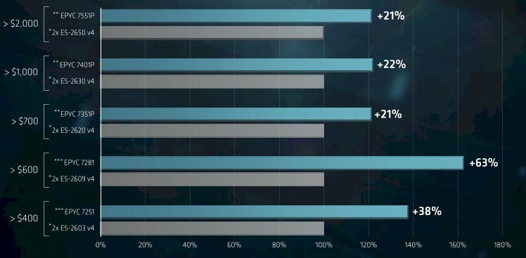
Here is how AMD thinks its Epyc 7000s in single-socket configurations perform on integer workloads, as gauged by the SPECint_rate_base_2006 part of the SPEC suite of CPU tests.
And here is how AMD did its comparisons for beefier two-socket configurations of the Epyc 7000s:
It is going to take some time to figure out if these comparisons make sense or not, and what we are really dying to do is make comparisons with the impending “Skylake” Xeons, which are due next month. But clearly, even with the performance gains we expect from Skylakes (around 8 percent or so improvement in instructions per clock plus more cores) AMD is going to still be able to compete against the Skylakes. Particularly if Intel doesn’t change its pricing.