


While AMD voluntarily exited the server processor arena in the wake of Intel’s onslaught with the “Nehalem” Xeon processors during the Great Recession, it never stopped innovating with its graphics processors and it kept enough of a hand in smaller processors used in consumer and selected embedded devices to start making money again in PCs and to take the game console business away from IBM’s Power chip division.
Now, after five long years of investing, AMD is poised to get its act together and to storm the glass house with a new line of server processors based on its Zen core, code-named “Naples” and now known by the Epyc brand, and a revitalized discrete GPU accelerator line based on its “Vega” generation of motors and sold under the Radeon Instinct brand. The change is an admission that modern workloads running on clouds, in hyperscale datacenters, and at HPC centers are as much focused on throughput as they are energy efficiency and that the accelerated processing unit (APU) CPU-GPU hybrids that AMD had been trying to get traction with in systems just didn’t have the necessary oomph to win deals. With APUs, AMD was telling customers to use many small sockets that, in the aggregate, provided great throughput at an affordable price and very good energy efficiency. But the market didn’t care. So now, with Naples, AMD is building a brawnier X86 socket (ironically from a multichip module derived from its Ryzen desktop chips) with a huge amount of memory and I/O bandwidth and for HPC and machine learning workloads the ability to directly them through PCI links to its own GPU accelerators, all running a clone CUDA environment and using a highly tuned compiler based on the LLVM stack.
This is story that better reflects the current computing market and that will probably resonate better. It had better, or the entire world will be calling this an Epyc Fail.
AMD has been very careful about revealing too much about the Naples Epyc and Vega Radeon Instinct compute engines, but ahead of the Naples launch scheduled for this week, the company has provided some strong hints about how it will try to take share away from Intel CPUs and Nvidia GPUs, which dominate their respective compute and accelerator portions of the datacenter.
Naples X86 server chips are set to debut this week at an event in Austin, Texas and we will be covering that launch as well as the happenings at the International Supercomputing Conference in Frankfurt, Germany. AMD lifted the veil a bit more on the Naples chips at its Financial Analyst Day last month, showing how its 32-core, 64-thread Epyc processors could best the current “Broadwell” Xeon E5 v4 processors from Intel and take on the impending Skylake Xeons, which are expected to launch sometime in July if the rumors are right. AMD is concentrating on the core two-socket segment of the market, and is convinced that given the performance of its single socket Epyc server chip and its ability to hang four or six Radeon Instinct coprocessors on the 128 lanes of PCI-Express 3.0 I/O bandwidth on a single socket that is can beat Intel in price and maybe on performance against a two-socket Xeon box that has GPU accelerators that require NVLink interconnects and PCI-Express switching hierarchy to attach to the Xeon compute complex.
We look forward into seeing how these various machines are priced and configured, and how they perform on a wide variety of simulation, modeling, machine learning, and database acceleration workloads. It is hard to judge without a lot more data, but at least AMD is in the game, competing again, and bringing to market the kinds of components that companies are familiar with and already buying from the likes of Intel and Nvidia.
Getting IT organizations to trust AMD again, as they did back in the middle 2000s, will be a bit of a challenge. And to help build confidence, the company has been talking a little more openly about its CPU and GPU roadmaps, and presumably is putting these out there and will not, as in days gone by, change them when the going gets tough. The company’s top brass talked about the impending CPUs and GPUs and put stakes in the ground for the following two generations. The details, mind you, are a little thin.
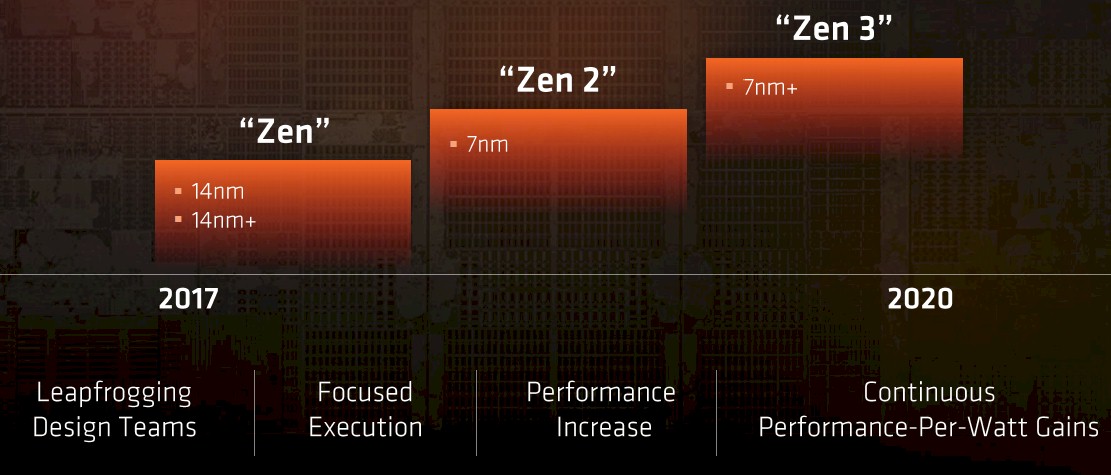
On the CPU front, AMD chief technology officer Mark Papermaster told the Wall Street crowd a month ago that the Zen 2 core has been in development for more than a year and that a Zen 3 core was in the works now that the original Zen core was coming to market. The current Zen cores are implemented in the 14 nanometer processes from foundry partner (and former AMD business) Globalfoundries, and a follow-on 14+ nanometer rev on this process will be used to goose the performance and yields on the Zen designs embodied in the Ryzen and Epyc processors. The Zen 2 cores, as the roadmap above shows, will be etched in a 7 nanometer process that Globalfoundries has started to talk about publicly (we are doing a deep dive on that now) and the Zen 3 chips will be created using a 7+ nanometer kicker technology and will not involve a process shrink to 5 nanometers or smaller. (IBM, which is a foundry partner with AMD and Samsung, has just demonstrated that it can do 5 nanometers in the labs and this tech, if perfected, can be adopted by Globalfoundries for future chips.) The three Zen cores will span a period from 2017 through 2020 inclusive, which is three core generations across four years, and that works out to an average of 14.5 months between generations if Zen 3 chips have an end of life in December 2020. That is a fairly brisk cadence, and we concede that the charts may not reflect planned, much less attained, timing for Zen core design rollouts.
As for the Epyc family of processors, the roadmap has a similar cadence, as you might expect.
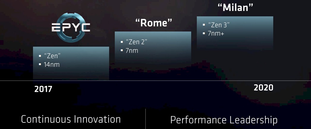
The first generation of “Naples” Epyc server chips will use the plain vanilla 14 nanometer processes from Globalfoundries, and it looks like the kicker 14+ nanometer technique is not going to be used in the next chip in the Epyc line, which is code-named “Rome,” or a follow-on Naples kicker. This Rome chip will use the Zen 2 cores and will be manufactured using the 7 nanometer processes at Globalfoundries, and the “Milan” third generation Epyc server chips will employ the 7+ nanometer techniques to make the Zen 3 cores and their adjunct components on the die.
AMD is not being specific about what it will do as it etches these follow-on Rome and Milan chips, but if the four-way multichip module design used for the Naples chips experiences latency and bandwidth issues on certain workloads (as we suspect it might), then AMD might be flush enough with cash to do a true monolithic design to get around these issues. That might radically increase the cost of making Epyc chips while only improving performance modestly, so we reckon that if AMD went with the chiplet approach to begin with, it might be hesitant to change strategy. It might make sense to create a special part if the performance of the Infinity fabric within the Epyc chip package creates a barrier to adoption for certain workloads. The point is, AMD could not do this on the first go around with Epyc, but if it starts making money with system chips, its options widen out and it can architect chips to take bigger slices away from Intel and possibly reach its natural 10 percent to 15 percent market share.
On the GPU front, AMD has been pretty tight lipped about the Vega GPU and the features it has for datacenter compute, but at the Financial Analysts Day, Raja Koruri, senior vice president and chief technology officer in charge of the newly composed Radeon Technologies Group at AMD, gave some details along with Papermaster.
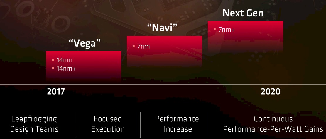
The plan and the processes are much the same as with the GPUs as with the CPUs. The “Vega” GPUs will start to roll out this month with a special Frontier Edition aimed at early adopters and enthusiasts, and these are made using the same 14 nanometer processes as the CPUs. There is a kicker 14+ nanometer process bump for the Vega GPUs, and then the “Navi” GPUs roll out in what looks like early 2018 from the roadmaps using 7 nanometer processes. The “Next Gen” GPUs that follow Navi don’t have a real code name yet, but they will use the 7+ nanometer node from Globalfoundries, and there are leapfrogging design teams to keep the innovation moving ahead.
To give a sense of the potential performance of the Vega-based Radeon Instinct coprocessors, AMD grabbed the DeepBench neural network training benchmark developed by Chinese hyperscaler Baidu and ran it on a system configured with a single card. This machine was able to train a particular machine learning model in 88 milliseconds. A single “Knights Landing” Xeon Phi 7250 accelerator (or host) was able to do the task in 569 milliseconds, by comparison, and a Tesla M40 accelerator based on Nvidia’s Maxwell GPUs did it in 288 seconds and a more recent Tesla P100 based on the Pascal GPU did it in 122 seconds. The Volta GPUs could offer substantially higher performance than the impending Radeon Instinct, but these tests show that AMD is in the ballpark and playing ball instead of being stuck in traffic a few miles from the stadium as it has been for many years in datacenter compute.
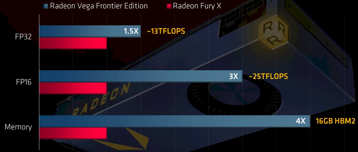
The Vega chip has 4,096 stream processors organized into 64 compute units, and is expected to deliver 483 GB/sec of bandwidth into and out of the double-stacked HBM2 memory; it comes in 300 watt air-cooled and 375 watt water-cooled. The Vega GPUs will have 16 GB of HBM2 memory on the interposer, and interestingly, have dedicated NVM-Express ports that will allow for 2 TB of flash capacity to be directly attached to the GPU accelerator to extend that memory size; think of it as a fast cache for the GPU memory. That HBM2 memory is four times as much as was crammed onto the prior Radeon Fury X GPU accelerators based on the “Polaris” GPUs, and with the support for half-precision FP16 floating point math, the devices will deliver around 26.2 teraflops of performance suitable for many machine learning training workloads. AMD is telling customers to expect around 13.1 teraflops of performance at single precision for floating point, and it has not talked about double precision performance. It is not necessarily going to be the case that double precision will be half of single precision (this happened with Nvidia’s “Maxwell” GPUs), and in fact with the first iteration of Vega chips, the scuttlebutt is that they will only offer double precision at 1/16th the rate of single precision. So that leaves the Vega accelerator at only 819 gigaflops at double precision.
The word on the street is that the kicker Navi GPU (which used to be called the Vega 20 in some roadmaps) will offer double precision at half the single precision rate when it comes to market in 2018. That shrink to 7 nanometer processes, using the same 4,096 streaming processors and 64 compute units, will increase performance by around 20 percent or so, which means single precision will be around 15.7 teraflops and double precision will be around 7.9 teraflops. AMD could shift to four stacks of HBM2 memory for a total capacity of 32 GB, and bandwidth could double or more, depending on a lot of issues with regard to memory speed, power draw, and heat dissipation.
For the sake of comparison, the “Volta” GPU accelerator from Nvidia that was just launched in May and that will be shipping in volume early next year, delivers 15 teraflops at single precision and 7.5 teraflops at double precision, and has special and additional 16-bit Tensor Core tensor processing units that can deliver 120 teraops of performance on machine learning training algorithms. AMD’s Vega GPUs do not have anything like the Tensor Cores, and from what we can tell, they do not have anywhere near the 900 GB/sec of HBM2 memory bandwidth across that 16 GB of memory like Nvidia does, either. There is also not anything like NVLink interconnects, but given AMD’s vast experience with APUs, we do expect coherency of memory across the GPUs and the CPUs, and if this does not happen, then AMD should know better.
Here is the point, however. We expect that AMD will be very aggressive on price with the Naples Epyc processors compared to Intel’s Skylake Xeons, and competitive with the Broadwell Xeons that Intel will use as a firewall for companies that don’t want to pay the Skylake premium that we think Intel will try to extract from the market while it can. The same tactics will play out with the GPUs. Nvidia list price was around $10,500 for a Tesla P100 Pascal-class accelerator, and let’s say for fun that the Tesla V100 accelerators cost $13,000 because the same math works backwards from the DGX-1 update. At those prices, even without a Tensor Core unit and even without decent double precision performance, AMD can take some share away from Nvidia where FP16 and FP32 dominate the workloads.
It can also make a less complex and less expensive CPU-GPU node, as the following chart illustrates:
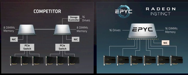
With a current system like Nvidia’s DGX-1, a cluster of GPU accelerators are linked to each other using NVLink, which provides memory concurrency across those GPUs. But because Intel does not support NVLink ports on its Xeons or their chipsets, it takes a pair of PCI-Express switches to link a pair of clusters of GPUs to a pair of CPUs and to the outside world with a pair of Ethernet or InfiniBand controllers. In the DGX-1, there are eight GPUs, not six shown in the diagram above, and with Volta they can all be cross-connected with NVLink; with Pascal Teslas, which has one fewer NVLink port, you have to use a mix of PCI-Express and NVLink to hook them all together. You also need a storage controller if you want to link flash SSDs to the compute complex, or burn PCI-Express slots using NVM-Express (which is not shown in the chart above). Because of the limited PCI-Express 3.0 lanes on each Xeon processor socket and the main memory cap per socket, you need a two-socket server to get the right mix of I/O and memory bandwidth and memory capacity.
Contrast this with a single-socket hybrid Epyc-Radeon Instinct system. The single socket machine has enough PCI-Express (Infinity Fabric) bandwidth to hang 16 flash drives and 16 memory sticks off a single socket plus six Radeon Instinct GPUs. That is the same memory capacity as an HPC-configured, two-socket Xeon server. The 32 cores on the Epyc die are probably enough to drive six GPUs, just as 32 cores would be on a two-socket Xeon server using a pair of 16-core chips. But there are only enough lanes in the Epyc system to drive eight GPUs total – and that is if there is no other networking or peripherals attached. It is not clear why each GPU does not have its own directly attached flash SSD as is possible with the Radeon Instinct accelerators, and in a balanced setup, some flash drives might be dedicated to the CPU and others to the GPUs.
With the lower cost AMD CPU and GPUs, plus the integrated chipsets and the fact that there are fewer sockets, it is hard to imagine the AMD box not having the same or better bang for the buck. (We think that it will be a lot lower, especially if Intel jacks up prices on Skylake Xeons as we expect it to.) Even if hybrid AMD systems only deliver 75 percent of the performance, but do so at half the cost, the company can very likely sell the components in such machines at reasonably high margins and drive both its top line and bottom line. This, we think, is the AMD strategy, and it is one that is designed to get AMD market share over the longer haul.
The trick will be to sustain the gap and shoot through it, and that depends on what system makers, who don’t want to annoy Intel, do and when and how they do it.