


One of the breakthrough moments in computing, which was compelled by necessity, was the advent of symmetric multiprocessor, or SMP, clustering to make two or more processors look and act, as far as the operating system and applications were concerned, as a single, more capacious processor. With NVLink clustering for GPUs and for lashing GPUs to CPUs, Nvidia is bringing something as transformative as SMP was for CPUs to GPU accelerators.
The NVLink interconnect has been in development for years, and is one of the “five miracles” that Nvidia CEO and co-founder Jen-Hsun Huang said at the GPU Technology Conference a month ago had to come together to make the “Pascal” GP100 graphics chip possible.
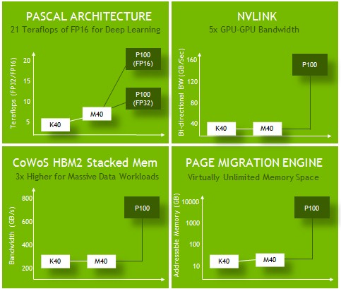
The other miracles include the Pascal architecture itself, which supports 16-bit half precision floating point math, important for machine learning algorithms and which has lots of tweaks to make use of NVLink.
Another is the shift to 16 nanometer FinFET processes from the 28 nanometer manufacturing techniques used for the “Kepler” and “Maxwell” GPUs; Nvidia skipped the 20 nanometer node at Taiwan Semiconductor Manufacturing Corp, which was perhaps unfortunate because Maxwell could have possibly been a better success for Tesla accelerators had it been available using 20 nanometer processes and filled in some gaps as the market awaits volume shipments of Pascal-based Tesla P100 accelerators in the first quarter of 2017.
The other risk that Nvidia took was for High Bandwidth Memory 2 stacked memory integrated with the Pascal GPU through chip on wafer on substrate, or CoWoS, packaging. The final miracle cited by Huang was improved machine learning algorithms that will be able to make use of up to eight interconnected Pascal GPUs that have shared virtual memory across the CPUs and GPUs in a node thanks to NVLink. That’s not really a miracle of technology, but rather the normal progress of software taking advantage of hardware, which always takes some time.
This high-speed, shared virtual memory, which will get cache coherency with the NVLink 2.0 that will launch with the “Volta” GV100 GPUs that are expected to launch in 2017 (probably later in the year, but we may get a preview at the GPU Technology Conference that year), is not something that Intel is offering to link multiple “Knights Landing” Xeon Phi processors or coprocessors together.
Intel certainly has the knowledge to allow for either SMP or NUMA linking of chips like Knights Landing and does NUMA links for its Xeon E5 and Xeon E7 processors that are pretty efficient. But as Intel told The Next Platform last year, it cannot off NUMA clustering on Xeon Phi chips because the memory bandwidth on the near and far memory in the chip, which will be in excess of 490 GB/sec combined, is so high that even modest snooping across the NUMA links would swamp any QuickPath Interconnect (QPI) channel linking two Knights Landing chips together through shared memory. We are not saying that Intel can’t – or won’t – come up with something like NVLink for hooking accelerators together, but the idea thus far seems to be to present Xeon Phis as processors in their own right and then to get high bandwidth interconnects – Omni-Path running at 100 Gb/sec and then in 2018 or so at 200 Gb/sec – linking the single-socket nodes together a little more loosely than the NVLink offers.
As we have discussed in our Future Systems series last year, Intel looks like it will be making increasingly smaller compute elements on Knights processors with higher memory capacity and bandwidth, while the OpenPower partners IBM, Nvidia, and Mellanox Technologies are creating hybrid CPU-GPU nodes with much more compute in aggregate and various memories that are shared in a virtual manner. Architecturally, both approaches have their elegance and practicality, and it will be interesting to see what real-world customers can do with them given their existing HPC codes. We think there is a chance that Intel will be able to do some things with Knights processors for machine learning, too, as Nvidia has done, but not having FP16 support in the Xeon Phi is going to be an issue, as we have already discussed.
NVLink Is Not CAPI
The problem with the PCI-Express bus is that it is a bottleneck in a hybrid system that mixes and matches CPUs and other elements, be they GPU, DSP, or FPGA accelerators or even memory devices like flash cards. So even with unified memory and with direct memory access across the bus, PCI-Express just doesn’t have enough bandwidth for unified memory architectures running at the very high bandwidth of devices like the Tesla P100 card, which delivers 720 GB/sec of memory bandwidth into and out of the Pascal GPU in its current iteration.
With the Tesla GV100 cards based on the future Volta cards, Nvidia has said it is targeting around 1 TB/sec of memory bandwidth. (This was divulged as part of the CORAL supercomputer award with the US Department of Energy for the “Summit” and “Sierra” systems.) This is a reasonable boost in bandwidth, but not as large as the double precision floating point performance will be from Pascal to Volta, we think. In any event, clearly something with more bandwidth than PCI-Express 3.0 or 4.0 is necessary unless someone wanted to gang up PCI-Express ports. (This might have been a simpler solution, and was probably contemplated.)
Even still, both IBM and Nvidia want to retain some of the PCI-Express programming model, whether it is the Coherent Accelerator Processor Interface (CAPI) for the current Power8 and future Power9 processors or Nvidia with its Pascal and Volta GPU accelerator cards because PCI-Express is something people know how to work with. In a sense, both CAPI and NVLink are specialized versions of PCI-Express. IBM leaves the underlying PCI-Express hardware alone and provides abstraction layers in its firmware and its chips to make CAPI devices look like they plug into a “hollow core” on the CPU and act like any other core when it comes to addressing shared memory. Nvidia has provided a much higher bandwidth interconnect than is available with PCI-Express 3.0 and is even better than PCI-Express 4.0 and will widen the gap more, we presume, with its second NVLink iteration.
If Nvidia it didn’t offer a substantial performance advantage, there would be no point to it. Nvidia would just embed a PCI-Express switch on the GPU and be done with it.
There was been some confusion about the bandwidth of the NVLink interconnect, and part of that is on Nvidia, whose presentations in 2014 and 2015 provided bi-directional bandwidth numbers for PCI-Express 3.0 links but only showed the uni-directional bandwidth of NVLink and PCI-Express even though the graphics indicated bi-directional links. Like this one from the Summit and Sierra supercomputer announcements from November 2014:
This left many of us scratching our heads about why Nvidia was so excited to have 20 GB/sec of peak bandwidth with NVLink 1.0 besting the 16 GB peak bandwidth of a PCI-Express 3.0 x16 port that would be normally used to support a Tesla accelerator card. Having 25 percent more peak oomph is great, but it is not earth shattering.
It turns out, Nvidia’s first iteration of NVLink is providing 40 GB/sec of bandwidth per link, if you do it bi-directionally, and when I originally wrote this story, I said this was significantly higher than 16 GB/sec of the PCI-Express link and did not understand that PCI-Express 3.0 delivers 32 GB/sec bi-directionally and thought the performance gap between NVLink and PCI-Express was more like a factor of 2.5X instead of 20 percent. In any event, two years ago many of us assumed that the excitement was around being able to gang up as many as four of these ports together to make a virtual uber NVLink pipe between two devices (that gives you the 2.5X in bandwidth that you crave). With PCI-Express 4.0, which debuts with IBM’s Power9 chip next year and which does not appear to be in Intel’s “Skylake” Xeon E5 v5 chip next year, peak bandwidth will be of 32 GB/sec over sixteen lanes each way, for a total of 64 GB/sec. We think that NVLink 2 will provide a bandwidth bump, but got the distinct impression that the number of NVLink ports would not necessarily increase on the GPU cards in the Volta generation. Our guess is to expect a 20 percent delta again between NVLink and PCI with the next generations of those protocols.
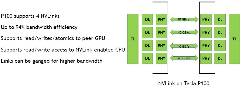
With the first generation of NVLink, the Nvidia Highspeed Signaling (NVHS) interconnect sends data between two devices over a differential pair that operates at 20 Gb/sec. Eight of these pairs are glued together for each direction, forming two sublinks that make up the NVLink and provide 40 GB/sec of peak bandwidth between two devices. The multiple links can be ganged up with two, three or four in a bundle, delivering 80 GB/sec, 120 GB/sec, or 160 GB/sec of bandwidth between devices.
With the Power8 chips now being enhanced with NVLink ports – don’t call it a Power8+ chip because it is not that even though IBM’s roadmaps from last year said there would be a Power8+ upgrade – companies interested in examining the potential uses of brawny hybrid CPU-GPU nodes can start to play with their code on such machines. But it does not take a CPU equipped with NVLink ports to make a more efficient GPU processing complex, as Nvidia’s own DGX-1 server illustrates perfectly. Take a look:
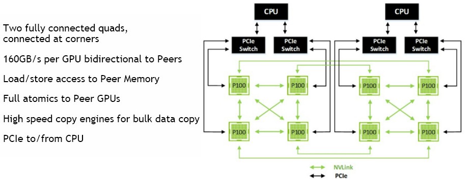
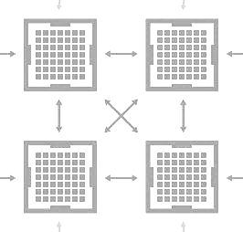
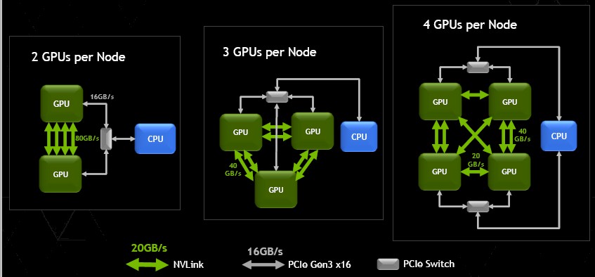
Each Pascal P100 card has four NVLink ports, and as you can see these can be used to directly link four GPUs to each other using three of the ports with the fourth port being used to link two sets of quads in a hybrid cube mesh architecture. With this approach, a GPU is no more than two hops away from any other GPU, and five eights of the time a GPU is only one hop away from any other GPU. But this hybrid cube mesh does not leave a way for the CPUs to link to the GPUs. Intel Xeon and IBM Power processors, which tend to be used in HPC settings, have their own on-chip PCI-Express controllers, which would enable linking the CPUs directly to specific GPUs in the system, but Nvidia’s approach with the DGX-1 system (and one that we expect other server makers to follow some of the time) is to put four PCI-Express switches from PLX, a division of Broadcom, onto the system board and link one CPU to half of the Tesla P100 complex and the other CPU to the other set of Teslas. (Some diagrams from Nvidia show only two PLX switches in the system, but the machine shows four switches, so we are going with four.) It is interesting to see that the switches are not used to cross couple the CPUs to each other, but this is done over QuickPath Interconnect and NUMA links over Power8 chips.
The NVLink connections at 40 GB/sec are obviously 2.5X faster than the PCI-Express links at 16 GB/sec, and the assumption that Nvidia is making is that connecting the GPUs so they can share memory and data is more important than passing data back and forth between the CPUs and GPUs, which will also happen thanks to the unified memory space implemented in the CUDA 8 environment and assisted by the page faulting hardware in the Pascal GP100 GPU. It is not entirely clear how data will be pinned to specific GPUs and CPU-GPU complexes and what routing will be used by the system to access data from CPU memory and GPU memory; it is also not clear how CAPI-enabled devices will plug into the unified memory between the CPUs and GPUs.
The Power8 chip is being equipped with NVLink ports precisely to give programmers a chance to play around with this hardware, and Nvidia has created its own DGX-1 system and is doling them out to researchers for the same reason. There is lots of automated memory management going on under the covers, and now the industry will find out how to program on top of it.
Intel does not and almost certainly will not add NVLink support to future Xeons, so PCI-Express ports hanging off the server and PCI-Express switching will be the way to link Xeons to Tesla P100s. For the Power8 machines, Nvidia is suggesting that a mix of NVLink and PCI-Express 3.0 ports be used thus:
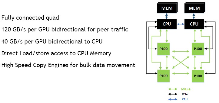
With this setup, a pair of CPUs is linked to each other and sharing main memory over a NUMA link. Each CPU is connected directly to a pair of Tesla P100 accelerators, using one port of NVLink running at 40 GB/sec and one link of PCI-Express running at 16 GB/sec. The GPUs are cross-coupled using the three remaining ports.
Interestingly, the modified Power8 chip has six NVLink ports, which means that, in theory, more complex nodes with different network topologies could be contemplated. It is not clear how the software stack Nvidia has created would deal with such topologies.
We think it would be interesting to show the performance of Tesla P100 accelerators in a system using just PCI-Express 3.0 x16 links and then turn on NVLink so customers can see the difference. Nvidia did not provide such data, but it did provide some performance comparisons against straight CPU systems to show the effect of using NVLink with Pascal accelerators.
In this comparison, Nvidia is showing the performance of a molecular simulation running in AMBER on a system with one, two, and four P100 cards, in the upper left. The scale shows the number of nanoseconds of movement for the molecule that can be simulated per day of system runtime. This is compared to the same AMBER simulation running on the Comet supercomputer at San Diego Supercomputing Center with a rising number of Xeon processors.
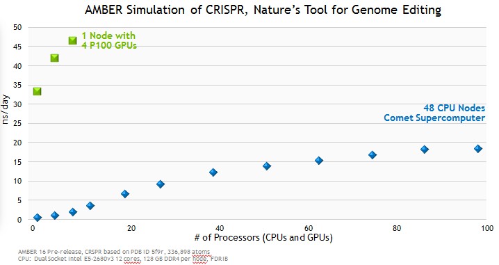
As you can see, the CPU cluster starts to run out of gas at 96 processors, at around 20 nanoseconds per day. A single hybrid node with four P100 accelerators can do 46 nanoseconds per day, and is probably a lot less costly, too. (Maybe on the order of one quarter the price, we speculate, if an average two-socket Xeon server node costs somewhere around $5,000 using the twelve-core Xeon E5-2680 v3 processors that are in the Comet machine.) If those prices are reasonably accurate, then the price/performance of that four GPU system is 8.5X better than the CPU-only cluster just at the raw compute level. Of course, what we want to know is how a node with eight GPUs might perform, and then how multiple nodes linked by a fast InfiniBand or Ethernet interconnect would do beyond that.
Our guess is that an eight GPU system based on Pascal accelerators would start to taper off, and that performance would get even flatter still over a cluster of such machines, but the numbers in the following chart don’t tell us the case for AMBER, which was only tested to four Tesla cards rather than eight. Anyway, take a look at this NVLink scalability chart for increasing numbers of Tesla P100 accelerators on various benchmarks compared to a two-socket Xeon server using the Haswell Xeons mentioned above.
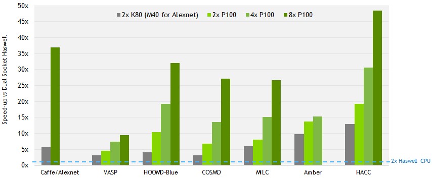
As you can see, the speedup of the Tesla accelerators varies quite a bit by application, and the performance boost compared to a pair of Tesla K80 accelerators is substantial. This is due to the combination of all of the features of the Pascal architecture, HBM2 memory, and NVLink all working together. Again, it would be interesting to isolate the effect of NVLink by itself, but Nvidia is selling this as a complete package and no one will be buying a P100 and not using NVLink. But down the road, when other Pascal cards are out, they might be looking at price/performance and decide that directly linked GPUs over PCI-Express 3.0 links are fine for their workloads and their budgets. We estimate that the Tesla P100 costs around $10,500 a pop, compared to around $3,200 street price for a Tesla K40 and $4,500 for a Tesla K80.
No matter the workload, what Nvidia and its server partners will be stressing is that the Tesla P100 offers huge benefits in performance and performance per watt over CPU-only clusters. Here is one such comparison, showing how many racks of servers it takes to match a rack of Tesla P100s on various applications and how much electricity those systems would consume:
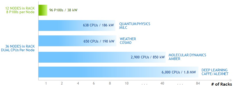
Those dozen DGX-1 nodes would cost $1.55 million, and you would be hard pressed to get your hands on them. So this is largely theoretical until early 2017, when the Tesla P100s are shipping in volume. And don’t get the wrong impression from this chart that the applications are scaling across that iron. This is just aggregating the performance of the benchmark results shown in the relative performance chart above. In other words, this is a capacity statement, not a scalability statement, for thinking at the rack level. Most clusters in HPC and in machine learning are run in this fashion – no one expects to scale applications across hundreds of GPUs or thousands of CPUs except in the most exotic settings.