


Moore’s Law might be winding down in observable ways, but that realization will not keep Intel from putting its maintenance on the front burner. It has been throwing a lot of core hours behind the engineering effort for the forthcoming 10 nanometer process, and is burning a lot of compute on solving the challenges that lie ahead on the path to 5 nanometers.
Although the company’s CEO, Brian Krzanich, has publicly stated that Moore’s Law is slowing in the wake of the company’s decision to push back availability on their ten nanometer chips by six months this summer, some at the company are fighting the idea that the continued, decades-long upticks in regular performance will end anytime soon. The key to keeping pace with Moore’s Law is working with the upcoming extreme ultraviolet technology (EUV), which will reduce the wavelength range necessary to move circuit designs onto silicon via masks, as well as a shift to 450-millimeter wafers within the next few years. As it stands now, too many hurdles with EUV stand in the way for it to push the 10 nanometer chips, but Intel is expecting this to change for future generations—including five nanometer (since they are skipping their former plans to move into full production with seven nanometer on EUV, according to TSMC’s CEO in an investor call over the summer).
It is no secret that the company is aggressively pursuing the five nanometer course, but according to Mark Bohr, Intel senior fellow in the Intel processor technology team, Moore’s Law is alive and well—and the momentum with five nanometer is a testament to that fact. “We continue to scale transistors, and each generation provides transistors that are higher performance, consume less active power, and cost less per transistor.” Bohr still strongly believes, despite the fact that Krzanich said the trajectory of production, which used to be on the order of two years, is closer to two and a half.
Bohr has seen the struggle play before. Recall that similar lithographic challenges stood in the way of Intel rolling out the 14 nanometer chips. In fact, he has seen a good part of the course of Moore’s Law from inside Intel longer than almost anyone inside the company. Bohr has been with Intel for a striking 37 years, and still sees the way forward despite the admitted host of roadblocks.
Just as Intel has done with its work on Knights Landing and from what we understand about the future Knights Hill processors, there will need to be some “tricks” to keep the Moore’s Law pony hopping—or at least looking lively. “One of several key challenges is trying to pattern ten or seven nanometer dimensions using lithography tools that have a wavelength of light of 193 nanometers. We need special tricks there. Another is that when we manufacture these scaled transistors and interconnects, some of the thin films we use are only a few atoms thick, which presents other challenges.”
At some point, the number of tricks at ever-smaller scale will come to an end, spurring a new, unseen shift toward other processor technologies, but for now, Intel is hard at work simulating the materials and lithography problems of continued shrinks. All of this comes at a significant cost across the board within Bohr’s five nanometer group, including on the computational side. As Bohr shared during this year’s annual Supercomputing Conference (SC15) in Austin last week, they are lighting up the cores on their own #99 ranked on the Top 500 November 2015 list) 833 teraflop Haswell-based HP supercomputer to continue the fight against the Moore’s Law decline.
Bohr says it takes a million CPU hours to design the photomasks to pattern the integrated circuits at scale currently. “That is the price we have to pay to pattern ten nanometer dimensions using 193 nanometer light.
Intel, who is now the prime contractor on one of the largest upcoming supercomputers known (the 2018 “Aurora” system) is coming to first-hand terms with the value of having large-scale simulation and modeling resources at hand. During the Supercomputing Conference, he shared a chart showing how his division has had to scale its infrastructure to support the design and implementation of new process techniques, noting that having a supercomputer on hand allows Intel to keep exploring a wider range of future device options using different materials and structures that would be impossible with just lab experiments—the dominant method before 2005 as seen below.
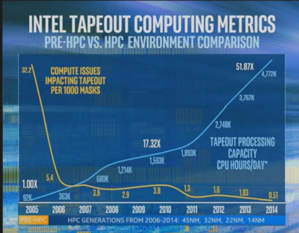
The blue line shows how Intel has increased compute power for future process design research since 2005. From that starting point until now, there has been a 50X increase. A slightly more nebulous line shows the corresponding increase in reliability, with failure rates dropping significantly, presumably as Intel has beefed up its own stack for HPC applications on partner iron.
Back in summer, 2015, the company’s Bill Holt, VP and GM of the Technology and Manufacturing group told investors that although the 14-nanometer process was behind schedule and projections at first, it has caught up with expectations, but Intel is keenly aware that the 22-nanometer process struck a sweet spot. “Our 22-nanometer technology is the highest yielding technology we’ve ever had. The bar that we’re trying to catch up to there is very high. That’s essential, because if you’re to get cost reduction, you have to match those other parameters of your previous generation.”
“We’ll always strive to get Moore’s Law back in two years,” said Brian Krzanich during Intel’s Q2 investor call in 2015. “And we’ll take a look at the maturity of EUV and the maturity of the material science changes that are occurring, the complexity of the product roadmap that we’re adding, ad make that adjustment out in the future.”