


The cadence of server processor launches by the remaining companies that still etch their chips has slowed in recent years, starting first with the low-volume players like IBM, Oracle, and Fujitsu and now possibly spreading to Intel with its Xeon line and already baked in with its Xeon Phi line with a roughly three year span between generations. This slower cadence is driven by a number of factors, the most important of which is that shrinking transistors on the Moore’s Law curve is getting more difficult.
Generally speaking, the chip industry thinks it can get down to 7 nanometers and still make chips that pack more transistors on a die and cost less per transistor. Last month, IBM and its partners Globalfoundries and Samsung Electronics demonstrated a test chip with transistors using silicon germanium gates and etched in 7 nanometer processes using extreme ultraviolet (EUV) lithography techniques. While these technologies have yet to be commercialized and tested at high volume, the fact that Big Blue and its partners demonstrated the technology at the 7 nanometer node gives its OpenPower partners and customers using Power processors today or thinking about doing so in the future (such as Google, which has said it is considering adopting Power chips for its workloads) confidence to invest in The Next Platform.
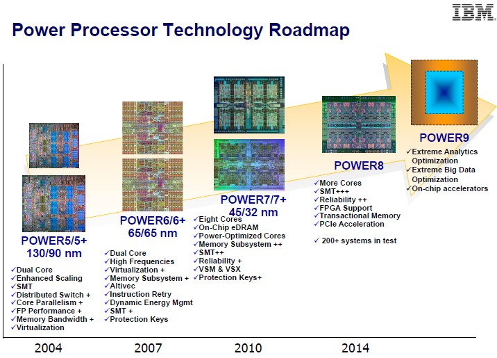
So does fleshing the roadmap out between the current 22 nanometer processes used with the Power8 chips and whatever those future 7 nanometer chips will be called. And to that end, IBM has been talking about its near-term plans for future Power8+, Power9, and now Power10 processors to select customers and government agencies. The company formalized and publicized its HPC roadmap at the ISC 2015 supercomputing conference in July, a roadmap we might add that The Next Platform told you about back in March. The latest Power roadmap we have seen puts some timescales and features on the future Power9 and Power10 processors, but still leaves plenty of details out chip roadmaps often do.
The official Power roadmap from IBM does not say much in terms of timing, but thanks to the “Summit” and “Sierra” supercomputers that IBM, Nvidia, and Mellanox Technologies are building for the U.S. Department of Energy, we knew Power9 was coming out in late 2017. Here is the official Power processor roadmap from late last year:
And here is the updated one from the OpenPower Foundation that shows how compute and networking technologies will be aligned:
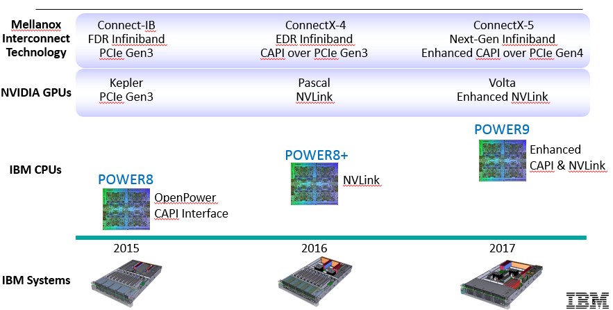
The interesting thing about these roadmaps is that the Power8+ processor will come out next year and will have NVLink high-bandwidth interconnects just like the forthcoming “Pascal” GP100 Tesla coprocessor from Nvidia. With NVLink, Nvidia is putting up to four 20 GB/sec ports onto the GPU coprocessor to speed up data transfers between the high bandwidth memory on the GPU cards and to improve the performance of virtual addressing across those devices. With the addition of NVLink ports on the Power8+ processor, those creating hybrid systems will be able to implement virtual memory between the CPU and GPU in an NVLink cluster without having to resort to IBM’s Coherent Accelerator Processor Interface (CAPI), which debuted with the Power8 chip last year and which offers similar coherence across a modified PCI-Express link. (That NVLink was being added to the Power chips was not obvious from prior roadmaps.) The future “Volta” GV100 Tesla GPUs from Nvidia and the future Power9 chips from IBM will sport an enhanced NVLink interconnect, which presumably will mean higher bandwidth and perhaps even a larger number of ports to link devices. A Pascal Tesla GPU will max out at four ports; it is unclear how many NVLink ports the Power8+ chip will have. IBM has also said that it will enhance its CAPI protocol to support PCI-Express 4.0 peripheral links with the Power9 chips.
IBM has not said much about the Power8+ and Power9 chips beyond these charts above, but the latest roadmap we have seen at least shows that the Power8+ chip will not include a jump to a new chip etching process, but rather will stick with the current 22 nanometer processes created by IBM and now controlled by Globalfoundries, which bought IBM’s chip business last fall.
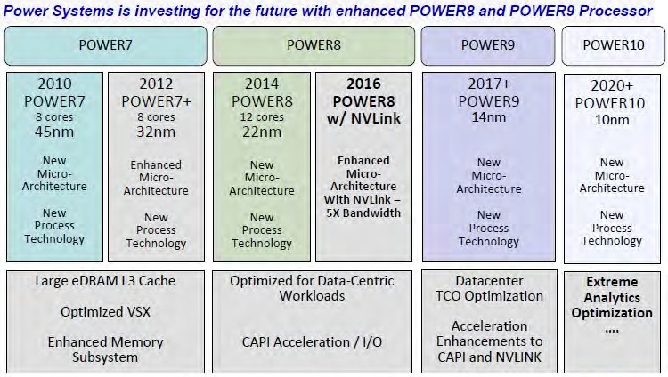
This roadmap above suggests that IBM will be enhancing the Power8 microarchitecture with next year’s Power8+ chip as well as adding in the NVLink interconnect support. Power9 is confirmed to use the 14 nanometer processes that IBM was working on by itself and which it has been enhancing with the help of Globalfoundries. That chip maker has a ten-year exclusive deal to supply IBM with Power and System z processors for its server line.
As for what Power9 chips will include, IBM has said only vaguely that it will have more on-chip accelerators and that it will be optimized for “extreme analytics” and “extreme big data.” We know from this latest Power roadmap that Power9 will include a new microarchitecture, and the other bit of news is that IBM will be optimizing the total cost of ownership for datacenter workloads. That could mean a lot of different things, from dropping chip prices as it has done for merchant versions of its Power8 chips to minimalist server designs that suit both hyperscale and HPC shops. But it is also guesswork at this point to try to suss out what IBM means.
We think that IBM could be adding some form of high bandwidth memory to the Power9 chip package, particularly variants aimed at HPC and hyperscale workloads that are not intended for multi-processor systems. But IBM has said nothing about its plans to adopt 3D stacked memory on its processors thus far, even though it has done plenty of fundamental research in this area. We also wonder if IBM will use the process shrink to lower the power consumption of the Power9 chips and perhaps even simplify the cores now that it has officially designated GPUs and FPGAs are coprocessors for the Power line. (Why add vector units if you want to offload to GPUs and FPGAs?)
What is new and interesting on the above roadmap is confirmation that IBM is working on a Power10 processor, which is slated for around 2020 or so and which will be based on the 10 nanometer processes under development at Globalfoundries. With the Power10, as with the Power7, Power8, and Power9 before it, IBM is changing the chip microarchitecture and chip manufacturing process at the same time. This IBM roadmap above does not show a Power9+ or Power10+ kicker, but both could come to pass if the market demands some tweaks to the microarchitecture around half-way between those three-year gaps between Power generations.
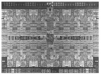
The cadence of the Power chip line suggests that we should not expect to see a Power11 chip, should one come to pass, using 7 nanometer etching techniques until around 2023 or so. All that IBM has said is that the transistor density that it expects from the 7 nanometer process will allow it to put 20 billion transistors on a future server chip. That’s about four times the number of transistors it can put on a Power8 die today using 22 nanometer processes. A whole lot of interesting things could be added to these future Power11 chips, including DRAM memory etched right along the processor cores. Why not? IBM has used embedded DRAM on the die as L3 cache memory since the Power7 generation back in 2010. It could happen, if there was some bandwidth and performance advantage.