

Hot on the heels of the closing of the deal that divests its semiconductor business and places it in the hands of Globalfoundries, the former chip making business of AMD that is controlled by the government of Abu Dhabi, IBM and its academic and chip industry partners have announced that they have successfully etched chips with transistors that are 7 nanometers in size – significantly smaller than current processes and extending the Moore’s Law curve one more step.
It is a big step, however, based on a mix of new technologies that have not been tested in volume production before, and IBM and partners Globalfoundries and Samsung Electronics are being very careful not to say when they will put the new 7 nanometer technologies to use making processors and other kinds of chips. The techniques that IBM and its partners have come up with use silicon germanium for portions of the transistors, which cuts back on power consumption for the very fast switching necessary for improving circuit performance, and the circuits are etched using extreme ultraviolet, or EUV, lithography, which may be difficult and expensive to put into production. EUV is very sensitive to vibration, as would be any technique that is trying to carve such small transistors onto a silicon substrate.
For decades, the Moore’s Law shrinking of transistors allowed not just for more transistors to be added to a circuit, but for those circuits to run faster within a certain power envelope and to be made more cheaply. This has enabled chip makers to add more and more components to their chips, in many cases integrating functions that would otherwise be on separate chips on a system motherboard into a single chip and in other cases adding whole new kind of circuits to their designs for running new types of applications. But about a decade or so ago, depending on the architecture, the thermal limits of systems imposed a clock speed limit on processors, and aside from some nominal instruction per clock (IPC) improvements with each microarchitecture change, clock speeds and performance for a processor stayed more or less flat. This is why CPU architectures went parallel, adding cores to expand throughput rather than increasing clocks to boost performance on a lower number of cores.
IBM had to actually pay Globalfoundries $1.5 billion to take over its IBM Microelectronics operations in East Fishkill, New York and Burlington, Vermont, mainly because its chip plants were not exactly on the cutting edge. The New York facility is capable of creating chips using 22 nanometer processes, which are used to make its latest Power8 processors for Power-based systems and z13 chips for System z mainframes. IBM was working on its own variant of 14 nanometer technologies as the deal with Globalfoundries went down and IBM Research and the microelectronics division were working together and with partners Globalfoundries and Samsung and chip-making equipment suppliers who collaborate through the SUNY Polytechnic Institute’s Colleges of Nanoscale Science and Engineering in nearby Albany to get a path to 10 nanometer and then 7 nanometer processes. The next node could possibly be at 4 nanometers, but no one is sure if this can be done in a way that is economically feasible. (The DNA in your cells is 2.5 nanometers wide, just to give you a sense of how small these circuits are getting.)
On the server front, Intel is beginning to ramp its “Broadwell” family of Xeon processors with its 14 nanometer processes, and is getting ready to being volume production of “Skylake” desktop and laptop processors using the same 14 nanometer process for later this year. Skylake Xeon processors will come to market in the 2017 timeframe, as The Next Platform has previously reported, and beyond that there are rumors of a “Cannonlake” successor that will shrink the Skylake to a 10 nanometer process. In the past, Intel has said that it thinks it has visibility to 7 nanometer processes, but like IBM has shown, has said that it may take a mix of materials other than pure silicon to accomplish this feat.
To help quell the fears of its Power Systems and System z customers and its new partners in the OpenPower consortium that seeks to open up the Power architecture and present it as a credible alternative to Intel’s Xeon processors in the datacenter, IBM announced a $3 billion, five-year effort to continue doing fundamental research in chip technology. This was while rumors were swirling around that IBM was not only interested in selling off its System x X86 server division to Lenovo Group, which it did, but also getting out of the chip manufacturing business. As part of its deal with Globalfoundries, IBM inked a ten-year, exclusive chip supply contract with the company for its Power and z processors. AMD still gets a lot of its processors from Globalfoundries, too, and so will benefit from the research that IBM, Globalfoundries, and Samsung are supporting to shrink circuits. Samsung has its own fabs and, like IBM and Globalfoundries, needs partners to shoulder the substantial economic burden of driving Moore’s Law.
IBM Research said that by using silicon germanium for transistor channels and EUV lithography, it was able to shrink transistor dimensions by 50 percent over the most advanced 10 nanometer techniques available today (in the lab, not in production chips), and added that this could result in a 50 percent better energy efficiency for the circuits. What IBM did not say is whether or not the cost per transistor would continue to come down using its processes, and basically it has to in order to justify the investment in the process.
For datacenters – because this all comes back to datacenters in one way or another here at The Next Platform – this issue is how the advances towards 7 nanometer technologies might preserve or even possibly speed up the Power processor roadmap. IBM has been quite clear that it wants Power chips to compete and win against Xeon processors in the datacenter, and showing that it can, through partnerships, keep pace with Intel, even if that partnership lags a bit just like massive foundry Taiwan Semiconductor Manufacturing Corp does, helps companies feel a little more easy about investing in Power technology. (TSMC makes processors for Oracle, Fujitsu, AMD, and a slew of the ARM server upstarts as well as for a number of switch chip makers, so it has a big play in the datacenter, too.)
When asked about the effect of the research on the IBM processor roadmaps, an IBM spokesperson gave the predictably vague answer. “The impact these chips will have on Power and z systems will depend on the needs of our IBM products, but we intend to incorporate 7 nanometer into the roadmaps for IBM systems in the future,” we were told. The technology is fully available to Globalfoundries as part of the chip fab deal with IBM, and presumably they will be working together to see how to commercialize it.
IBM has been pretty vague about the Power roadmap, too, but we have been able to piece some data together. Here is the official roadmap that IBM has been sharing with business partners and customers in the wake of the Power8 rollout in 2014:
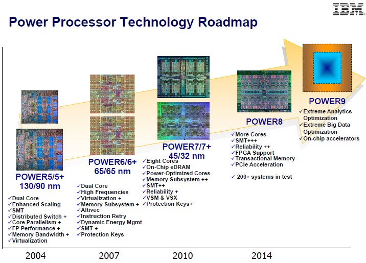
Way back in the dawn of time – well 25 years ago – when IBM launched the Power system line (it was called the RS/6000 back then), the RIOS-1 chips were implemented in 1,000 nanometer processes, but the Power4 generation in 2001, when IBM became a credible threat to Sun Microsystems and Hewlett-Packard in the Unix systems market that dominated the datacenter at the time, IBM had shrunk down to 180 nanometers and was able to put two cores on a die and still get the clock speeds up to 1 GHz to 1.3 GHz. At that time, IBM tried to stagger architectural changes and process changes, but had mixed results. The Power4+ shrink to 130 nanometers provided some clock speed boost, but was really a dry run for the chip making techniques that would be deployed on the Power5 two years later in 2004. The next year, IBM did a 90 nanometer shrink to Power5+ and used a mix of single-chip and dual-chip modules to goose the per-socket performance; clock speeds ranged from 1.5 GHz to 2.3 GHz, also helping to push up performance on the dual-core chips. With Power6, IBM moved to 65 nanometer processes and cranked the clocks up to between 3.6 GHz and 5 GHz, and the Power6+ was largely a dud excepting some dual-chip modules IBM got into the field to add more threads to each socket and offer better competition with Intel Xeon and AMD Opteron processors of the time. (AMD was the real threat back then.)
More recently, with the Power7 generation, IBM used the shrink to 45 nanometer processes to jump to eight cores per die and clock speeds of between 2.4 GHz and 4.25 GHz. The Power7 cores had a lot more oomph than the Power6 cores, and IBM brought embedded DRAM L3 cache onto the die as well, significantly boosting performance for many workloads. The Power7 chips also supported simultaneous multithreading, providing four virtual instruction threads per core. (Intel’s HyperThreading supports two threads per core and AMD does not support threads on its cores, or won’t until the Zen core in 2016 if the rumors are right.) The Power7+ shrink to 32 nanometers allowed IBM to boost the L3 cache to 80 MB (up from 32 MB for the Power7) while tweaking the clock speeds up a little. A majority of the 2.1 billion transistors on the Power7+ die are for this cache, in fact.
With the Power8 chips that rolled out last year, IBM was able to put 4.2 billion transistors on the die thanks to the shrink. That allowed it to boost the core count to twelve and the L3 cache to 96 MB as well as adding other features. (At 675 millimeters square, the Power8 chip is also 20 percent larger than the Power7 and Power7+ die, so that helps with the feature expansion a bit.) IBM also boosted the SMT to eight threads per core with the Power8 chip.
That leaves us looking ahead to what happens after Power8, and the OpenPower HPC roadmap provides some additional clues:
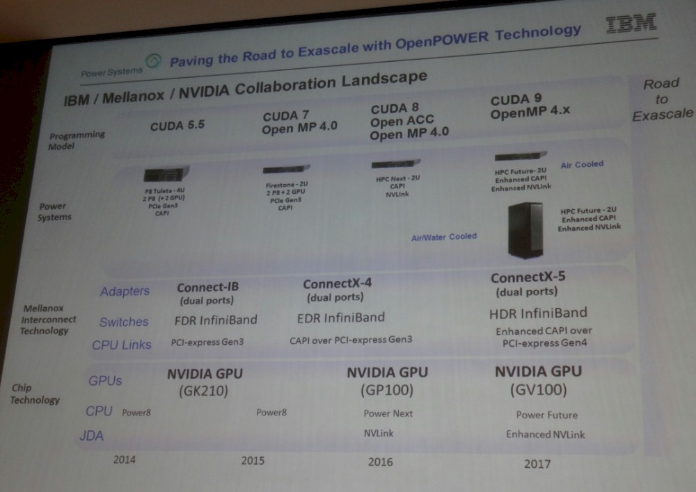
Thanks to the “Summit” and “Sierra” supercomputers that are being built by IBM, Nvidia, and Mellanox Technologies for the US Department of Energy in late 2017, we know for sure when the Power9 chip is coming. We also know that there is an interim Power8 chip that will support Nvidia’s NVLink technology for coupling GPUs tightly to each other and to CPUs for more efficient hybrid computing. The interim Power8 chip is, as you can see from the chart above and from our earlier coverage on the OpenPower HPC roadmap, is slated for 2016. We know from speaking to IBM last year, when the Globalfoundries deal was inked but not yet done, that IBM and Globalfoundries were working on a hybrid 14 nanometer technology and that Power chips would be moved completely over to Globalfoundries’ processes by the 10 nanometer node. It is not at all clear if that future Power8 chip will be using the existing 22 nanometer technology created by IBM or this hybrid 14 nanometer technology.
In the past decade, IBM liked to have three years between major processor generations, squeezing a “plus” variant of the chip in there – sometimes with a process shrink and sometimes not – somewhere in the middle. IBM has not said much about the Power9 chip, but did concede back in the summer of 2013, when the first details were made available for the Power8 processor, that it had been working on the Power9 concepts already for quite some time. It is unclear how the advent of the OpenPower consortium and the needs of participants such as Google and Nvidia have changed that Power9 plan, if at all.
It is hard to guess precisely what processes will be used where, and that is because the nodes are getting tougher. There is a good chance that the Power8+ chip coming next year with the first pass of NVLink will use the 14 nanometer processes that IBM was already working on and that Power9 will use them as well. Power9 could go all the way to a 10 nanometer shrink as well, if IBM and the OpenPower partners want to be more aggressive and chase more HPC and hyperscale business and take a bigger bite out of the enterprise systems business, too. It seems far more likely, based on history, that a Power9+ chip, perhaps coming in 2018 or 2019, will use 10 nanometer processes, and then that a future Power10 chip will use a ramped 10 nanometer process. Wherever 10 nanometer processes are deployed, given a roughly same die size, a Power9 chip could have around 10 billion transistors – more than twice what is possible on the Power8 chip. (That is our math, not IBM’s.)
Now, IBM and its partners could add a lot more eDRAM L3 cache to such a chip and a lot more cores, or a lot more pipes directly out to non-volatile memory and other kinds of accelerators. There are all kinds of options with a transistor budget that large. With Intel expected to have up to 22 cores in the Broadwell Xeon E5s (we anticipate an announcement for these in early 2016 now, not later this year as many had been thinking) and up to 28 cores in Skylake Xeon E5s (perhaps coming in the summer of 2017 but no one can tell the timing yet), IBM and its OpenPower peers must be sorely tempted to boost the core count on the Power9 chips. There is certainly room to double it to 24 cores, if that is desirable.
The staggering thing to consider is what the move to 7 nanometers brings. IBM says it can get 20 billion transistors onto a server-class chip – nearly four times what it can do with Power8 chip etched in, and presumably on a significantly smaller die size than the current Power8 has. That is a tremendous amount of transistors. The forthcoming 72-core “Knights Landing” Xeon Phi processor from Intel weighs in at over 8 billion transistors, by comparison. This Knights Landing chip is using Intel’s current 14 nanometer processes, which are also being used on the Xeon D processor it created for hyperscalers and the future Broadwell Xeon E5 and E7 chips.
The upshot of all of this is that IBM and its OpenPower partners have a line of sight well beyond 2020 for Power10 and possibly for Power11 chips. That all depends on if this 7 nanometer process can be commercialized and brought to Globalfoundries’ chip plants in an economical and timely fashion.


Be the first to comment