


Having an annual cadence for the improvement of AI systems is a great thing if you happen to be buying the newest iron at exactly the right time. But the quick pace of improvement of Nvidia’s rackscale AI systems and the scale-out networks to massively embiggen them also means that at any given time, a certain portion of customers have buyer’s remorse and wished that they had waited.
This is arguably a first world problem, we realize, and not one worth whinging about when getting your hands on any GPU or XPU capacity at all is the real problem.
But still, as the world watches the keynote address of Nvidia co-founder and chief executive officer Jensen Huang at the Consumer Electronics Show 2026 in Las Vegas today, more than a few executives will no doubt be thinking “shoulda waited” as they see the feeds and speeds of the future “Vera” Arm server CPUs and “Rubin” GPU accelerators unveiled alongside the specs for the scale-up NVLink memory fabric and the scale-out Spectrum Ethernet interconnect rolled out alongside new NICs and DPUs to create a much-improved rackscale system for chewing on or spitting out tokens.
To be a tad bit more specific, Nvidia’s top brass says that the Vera-Rubin NVL72 rackscale system, which as the name suggests has 72 GPU sockets and that also has 36 CPU sockets as well as the NVSwitch fabric linking them all together, delivers a 10X reduction in inference cost per token for mixture of expert (MoE) AI models and a 4X reduction in the number of GPUs (but maybe not a 4X reduction in cost, be careful there jumping to the wrong conclusion) to train those models compared to the prior generation of Grace-Blackwell NVL72 systems. (This is comparing the GB200 NVL72 systems to what we presume will be called the VR200 NVL72 systems.)
Smoother Transition Than Blackwell
Nvidia launched its first homegrown server in April 2016 with the DGX-1 system based on its “Pascal” P100 GPU accelerator and a hybrid cube mesh of NVLink ports lashing together the eight GPUs in the system. This was a fairly simple machine by modern standards, and significantly the very first one was given to Sam Altman, chief executive officer of OpenAI.
Two years later, the DGX-2 platform came along based on the “Volta” V100 GPU and this funky little thing called NVSwitch, which was a research project out of Nvidia Research. With the DGX-2, Nvidia got its first taste of complex system component development and integration, and rather than let others build to a spec, Nvidia manufactured the GPU boards, switch boards, and planar interconnects between the two all itself to maintain quality control. The “Ampere” A100 and “Hopper” H100 GPUs had similar designs, pumped up to deliver more floating point oomph and bandwidth to support it, but with the “Blackwell” GB200 NVL72 designs launched in March 2024, Nvidia went rackscale and crammed 72 GPU sockets, 36 CPU sockets, and 18 NVSwitch trays into the “node” to create a shared memory system that was complex, hot, and a challenge to manufacture as well as in very high demand and very tight supply.
There were issues with the initial Blackwell rackscale machines, and that forced GPU and rack redesigns on several fronts, which of course meant delayed shipments – from late 2024 to early 2025 in reasonable volumes. But, when you are building the most complex server node the world has ever seen, pushing the envelope on integration and thermals, you have to expect for things to go wrong here and there, no matter how careful and thoughtful all the engineers are.
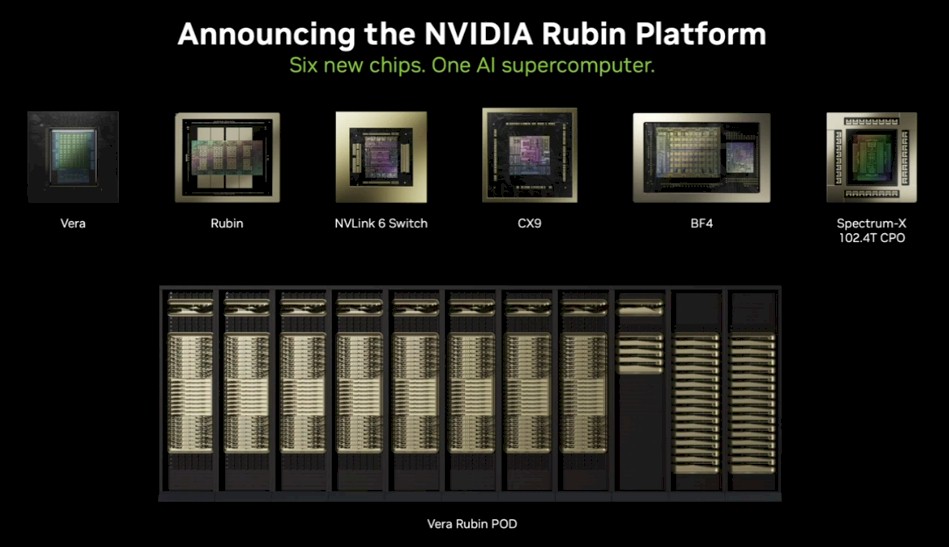
This time around, with the Vera-Rubin VR200 NVL72 machines, everything is on track. In a pre-briefing with journalists and analysts ahead of Huang’s keynote, Dion Harris, senior director of HPC and AI factory solutions, said that all six chips at the heart of the Vera-Rubin NVL72 platform were back from the Taiwan Semiconductor Manufacturing Co foundry, were being brought up and sent out to key partners and could start ramping production in the second half of 2026.
We strongly suspect that Nvidia will unveil a lot more details about the VR200 NVL72 platforms – these are counting GPU sockets instead of chiplets, so this machine is also what Nvidia had been previously calling the VR200 NVL144 systems in roadmaps from last year – at the GPU Technical Conference 2026 in San Jose in March. But for now, we will share what has been unveiled about the machines here at CES. (Or rather, there at CES, since we are home and not at the show because there are some family medical issues going on.)
Perhaps the most important chart that Harris showed in the prebriefing is this one, which shows why the design of the Vera-Rubin systems is heavily focused on getting HBM stacked memory bandwidth up so those very expensive Rubin GPUs can be better fed than was possible in the Hopper and Blackwell generations. (Just like you go to war with the army you have, not the one you wished you had, every IT supplier goes to market with the components they can integrate that have the highest reliability and the lowest possible cost.) Take a look:
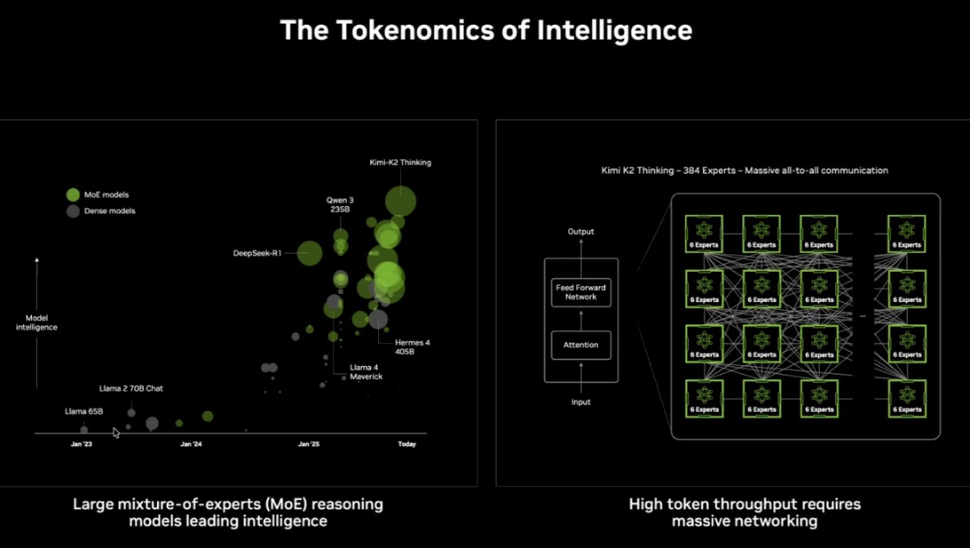
But in this mixture of experts era, models have to create and analyze more tokens to come up with better answers, and if you want to do that in a timely fashion, it takes massive bandwidth to handle all of the communication as different experts consult with each other.
And so, we think, the most important metric to consider in the new Vera-Rubin machine is that eight stacks of HBM4 memory in the Rubin GPU – presumably the R200, but Nvidia has not said its name as yet – have a combined 22 TB/sec of memory bandwidth, which is 2.75X higher than the 8 TB/sec of the eight HBM3E stacks used in the Blackwell GPU. This is a bit higher than expected, but the 288 GB of capacity, at 1.5X times the 192 GB in the Blackwell B200 GPU, is right in the mark. (Nvidia could create fatter memories in the future if HBM supplies loosen up, but we strongly suspect that will happen with the Rubin Ultra GPUs in 2027, not with the Rubins in 2026.)
Here are the basic specs for the Rubin GPU:
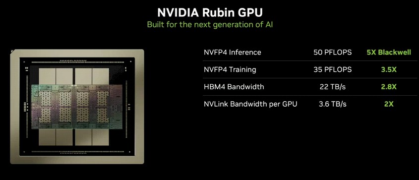
You will notice that the NVFP4 performance for inference on this two-chiplet Rubin GPU socket is rated at 50 petaflops, which is 5X the performance of the Blackwell B200 GPU, but that on training, the performance at the NVFP4 precision for floating point operations is only 35 petaflops, which is only 3.5X of the 10 petaflops of the B200. The follow-on B300 was tweaked to yield 15 petaflops for AI inference, which was a 50 percent boost over the B200. Nvidia never really explained how this happened.
But with the Rubin GPU, Ian Buck, general manager of hyperscale and HPC at Nvidia, there is an explanation and it is called adaptive compression, which is part of the redesigned tensor cores on the Rubin GPUs and that is part of the next-generation Transformer Engine that those tensor cores implement.
“Adaptive compression is a technique that is basically a smarter form of sparsity that is able to be applied adaptively and in a way that we know it doesn’t impact accuracy,” Buck tells The Next Platform.
While Nvidia has not said this, we strongly suspect that this is one of the key differences between the Balckwell B300 and the earlier B200 GPU. (This would not be the first time a technology was pulled from the future into an Nvidia GPU.) How else explain the 50 percent boost in inference performance with the B300? The clock speeds sure as hell did not get that much faster on a chip that was implemented in a 4 nanometer process.
We will dig further into the Rubin GPUs, but the Rubin complex has 336 billion transistors and we think is etched in TSMC N3 3 nanometer processes (although it could jump to 2 nanometer N2 processes), compared to 208 billion transistors for the B200. That is a 62 percent increase in transistors to deliver a 3.5X boost in performance without the adaptive compression boost – and we want to know how that happened.
On the CPU front, the AI and sometimes HPC platform coming later this year from Nvidia includes the Vera Arm-based CPU and Nvidia’s homegrown “Olympus” cores.
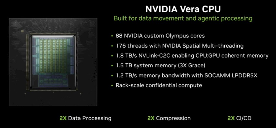
Vera is a much better CPU than was Grace based on the first glance that we are getting at CES. The Vera chip has 88 cores with two threads per core with what Nvidia calls “spatial multithreading,” which has yet to be explained.
The Vera cores have 2 MB of L2 cache per core (2X that of Grace and its not-custom Arm Neoverse “Demeter” V2 cores), and 162 MB of shared L3 cache across the cores (up 42 percent from the 114 MB of L3 cache on the Grace CPU). The Vera chip has 1.5 TB of LPDDR5X memory, which is 3.2X higher than the 480 GB of LPDDR5X memory on Grace. Each Vera core has six 128-bit SVE2 vector engines that support FP64 down to FP8 formats, which is neat, compared to the four 128-bit SVE2 units that supported FP64 down to FP16 formats in Grace. At 1.8 TB/sec, Vera has twice the NVLink shared memory bandwidth going into and out of it compared to Grace, which allows it to share data very quickly with the pair of Rubin GPUs it is paired with in an MGX system board that is the key component of the Vera-Rubin VR200 NVL72 system.
Put them together, and you have what Nvidia calls the Vera-Rubin superchip and what we would call a system board:

Put two of these into an MGX server sled and then eighteen of these sleds into an “Oberon” rack with 36 NVSwitch 4 switches (which Nvidia is now calling the NVLink 6 Switch to stop confusing people), and you have a rackscale system thus:

Considering that Nvidia has yet to start selling this Vera-Rubin beast, we have no idea what it costs. But given that everything in this rack is more expensive to make than its processor and that it clearly provides more oomph in the same space and a lot better performance per watt, we think Nvidia will be able to charge a premium for Vera-Rubin systems. How much, the market will decide – with some heavy input from Nvidia’s famous co-founder and chief executive officer, we expect.
If the GB200 NVL72 cost around $3.35 million, as we estimated it did two years ago, then with 5X the inference performance you would expect the VR200 NVL72 to cost $16.8 million. Ah, but the cost per token has to come way down, and Nvidia said that it would come down by a factor of 10X for MoE inference. So now you are down to $1.68 million. We do not believe for a second that Nvidia is only going to charge $1.68 million for a VR200 NVL72, and hence we do not know where that 10X reduction in cost comes from mentioned above. (We think it might be measured MoE inference performance, not the peak theoretical performance shown in the chart immediately above.) We have an easier time believing that Nvidia might charge 2.5X more money than the GB200 NVL72 for 5X more raw NVFP4 performance with the VR200 NVL72, which is around $8.4 million for 50 percent reduction in the cost of raw inference performance. A lot will depend on how much Nvidia can squeeze out profits. Considering how much trouble Nvidia had with Blackwell at first, and how smooth the transition might be to Rubin, there might be some room to cut prices lower than we expect to keep the competition at bay.
Some of that competition is coming from Nvidia’s lighthouse customers for Vera-Rubin systems, which the company said includes Amazon Web Services, Google Cloud, Microsoft Azure, Oracle Cloud Infrastructure in addition to smaller players such as CoreWeave, Lambda, Nebius, and Nscale. The first three customers are making their own accelerators, and Google can very likely do it at the same or a lower cost per token than Nvidia can at the hardware level – and build systems that scale to 9,216 TPUs in a single memory domain. This scale is a very big deal, and is the real engineering issue that Nvidia has to solve. We are convinced that it can do it, too.