


Pat Gelsinger, current chief executive officer at Intel and formerly the head of its Data Center Group as well as its chief technology officer, famously invented the tick-tock method of chip launches to bring some order and reason to the way the world’s largest chip maker – as it was in the mid-2000s – mitigated risk and spurred innovation in its products.
As anyone who has watched the semiconductor industry knows, changing both the design of a chip and its manufacturing process at the same time gives twice as many chances for things to go wrong. And things always go wrong. That is the nature of designing and making chips, and all of the simulation and multiverse in the world will not change that – although we strongly believe that the former has helped immeasurably in helping chip designers and makers get their products out the door in a reasonably timely fashion. In 2017, Intel created an augmented cadence that we called tick-tock-clock and that it called process-architecture-optimization, and we did not know our phrasing came from the 14th course in the Super Mario 64 video game.
At about that time, Intel’s 14 nanometer process was humming along and its 10 nanometer process was going to go up onto the rocks pretty hard, smashing both client and server CPU roadmaps and hurting other products like FPGAs and many-core processors and GPUs, too. That 10 nanometer process, which shows off the SuperFIN transistor design in its final incarnation, was arguably four years late coming to market and while competitive in many respects with the 7 nanometer processes from rivals Taiwan Semiconductor Manufacturing Co and Samsung Electronics, but the time the “Ice Lake” Xeon SPs were in the field in April 2021 using what the company called the Intel 7 process, AMD already had “Milan” Epyc 7003 processors in the field a month using true 7 nanometer processes from TSMC and has moved on to 5 nanometers with the “Genoa” Epyc 9004s and their derivatives and is gearing up for 3 nanometers this year with “Turing” Epyc 9005s and their derivatives.
Intel may be able to catch TSMC at some point – the promise that Gelsinger made was five nodes in four years, abbreviated to 5N4Y – and that is something that TSMC has said rather emphatically will not happen. So some arbitrator will have to judge. But if Intel can get something akin to process competitiveness and hold onto it, then its CPU, GPU, FPGA, and DPU businesses will have a much better chance of competing in the market than has been the case for the past five years, when Intel had a bunch of supply wins and a decreasing number of design wins compared to arch rivals AMD and Nvidia on the chip design side of the house.
But everything will not be back to the way it was after the 5N4Y goal is accomplished. Intel Foundry, formerly known as Intel Foundry Services, will be a freestanding business unit within Intel, and the divisions that design and sell their various kinds of devices that use the foundry will have to pay for manufacturing and packaging services and they will have to stand in line and get their allocations just like outsiders do. Their own profit and loss statements will be separate from those of Intel Foundry, and they will not have a nearly unlimited number of do-overs as they design and re-design those devices without consequences. Now, then every revenue dollar and every cost matters, Intel has not choice but to rein it all in and focus on making chips and designing chips – and getting it right the first time as rival TMSC does in manufacturing, thereby helping its downstream customers to get their advanced CPUs, GPUs, and other chippery into the field ahead of Intel, and usually with better performance and price/performance metrics these days.
There are exceptions to that statement, of course. In the datacenter, the “Sapphire Rapids” Xeon SPs have actual design wins thanks to an HBM2e memory option as well as to on-chip accelerators that allow a Sapphire Rapids chip with fewer cores than rivals to get the same amount of work done.
In the future that Gelsinger has been trying to create for Intel, the foundry will have to live by its merits and so will the chip product groups – and independent of each other in terms of P&L but absolutely dependent upon each other as any chip designer is with its foundry partner.
Intel can only be a foundry if it has more than one customer, and that means it must attract the likes of Nvidia, the Arm collective, Broadcom, and others such as the hyperscalers and cloud builders who are designing their own chips – often to get time to market and other advantages like lower costs and greater control compared to relying on Intel’s chips – to adopt its chip etching and packaging. And that means literally arming the competition with the best chip and packaging technology that Intel can bring to bear.
It may not look like it now, but in the long run, once the foundry business is stabilized, growing, and then humming along, it will be easier for Intel Foundry to get business – thanks to national manufacturing sentiments in the United States and Europe – than it will be for Intel to compete against AMD, Nvidia, and the Arm collective designing and peddling chips.
This may be the best thing to happen to Intel, or the worst thing to happen to Intel. Only time – and tens of billions of dollars in capital investment – will tell. But it does feel like this was the only thing that could happen to Intel, considering how both halves of the house were not operating properly.
Though it may be heresy to say it, in the long run, Intel may decide to spin one or the other half out. But it is far more likely that Intel will keep itself together, just like IBM did in the 1990s when it was all the rage to talk about breaking it up into Baby Blues when its several businesses also went up on the rocks and Big Blue had its own ”near-death experience,” as IBMers still call it to this day.
Anyway, without further ado, here is the latest Intel Foundry roadmap:
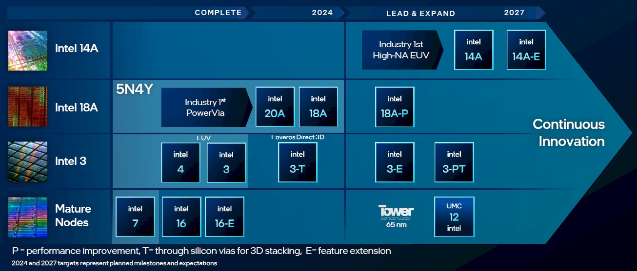
For the datacenter, the process nodes to watch are Intel 7, Intel 4 (not really), Intel 3, Intel 20A, Intel 18A, and the just-revealed Intel 14A and its Intel 14A-E extension. It looks like Intel 14A is coming around 2026 and the Intel 14A-E extension is coming in 2027.
Intel 7 and Intel 4 are in the market and have been for some time. Intel 7 is used to etch the fifth generation “Emerald Rapids” Xeon SPs, which launched in December 2023, and so was the prior fourth generation Sapphire Rapids Xeon SPs. The Intel 4 process, which in some ways in analogous to the TSMC 5N nanometer process, was supposed to be used on the future sixth “Granite Rapids” Xeon SP CPUs, nut Intel moved it ahead to the much smaller Intel 20A process, which is a 3 nanometer extreme ultraviolet (EUV) process like TSMC 3N. Intel will argue that in some dimensions the 5 nanometer Intel 3 process is more like a TSMC 3N 3 nanometer process. In any event, the future “Sierra Forrest” Xeon SPs, which have lots of E-cores instead of the fatter P-cores used in Granite Rapids, are also etched in Intel 3. The Intel 4 process was used for some client CPUs, but was skipped for datacenter stuff, namely because it is a 7 nanometer process that really can’t compete with the 5 nanometer and soon to be 3 nanometer processes that TSMC is bringing to bear.
The Intel 20A and Intel 18A processes, which will have Power-Via combined with gate all around (GAA) transistor designs, are on track, according to the company. The Intel 18A process is open for foundry customers to design to starting now, and will be ready for full product design in the second quarter. The P-core using “Diamond Rapids” Xeon SPs are slated to use either the Intel 20A or Intel 18A process, which is getting down into the 2 nanometer zone. The “Clearwater Forrest” kickers to Sierra Forrest are using 18A, so we see no reason why Diamond Rapids won’t, too. Why should the Xeon SP group pick up the tab for an inferior process and shoulder those costs? We wouldn’t. Not with Intel Foundry customers shooting for Intel 18A in 2025, as we suspect many will do.
The new thing on the roadmap is the Intel 14A process, which will be commercialized in late 2026 and according to Intel will be the first process to use High NA EUV technologies. While the High Numerical Aperture lithography technique allows for transistors to be shrunk, it also cuts the reticle limit in half, which means you can’t make a chip with as many transistors. This would argue for the inevitability of chiplet designs and also yet another transition in technology that chip designers have to cope with.
Side note: You know why IBM got out of the chip making business? Because its experts figured out that each new real node would eventually require a whole new technology at each and every process node. That’s tiock-tiock-tiock-tiock. . . out to infinity. That was not a game for making money at the kinds of volumes that IBM had for its mainframe and Power processors as well as the embedded stuff it was building at the time.
Things are not quite that bad yet, of course, because engineers are seemingly endlessly clever. But the jump to 2 nanometers and below has its own problems by cutting the reticle limit in half.
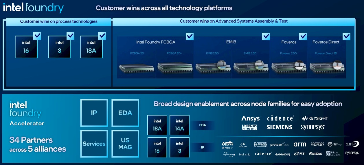
Which is why you should not count Intel out, either as a foundry or as a chip designer. And especially not as both at the same time. Clearwater Forrest has taped out using the Intel 18A process, and others are sniffing around and some are making commitments because having TSMC as the sole foundry that can do advanced packaging as well as advanced processes is too big of a risk. Especially with China having aspirations about Taiwan.
As we have pointed out before, by becoming less dependent on TSMC, we actually make it more likely that China will invade Taiwan. And also more likely that should this happen, it won’t be the multinational security risk that it undeniably is and perhaps we won’t all die as 12,512 nuclear fireballs are burnt around the surface of the Earth. Maybe we better just hope Intel makes it, and Samsung helps with its foundry, too. There is more at stake than a handful of $15 billion foundries and a few tens of billions of chips being etched. In fact, having Intel Foundry succeed is more important than having Intel Inside succeed as far as we can tell.