


Big Blue was one of the system designers that caught the accelerator bug early and declared rather emphatically that, over the long haul, all kinds of high performance computing would have some sort of acceleration. Meaning, some kind of specialized ASIC to which a CPU would offload its math homework.
Maybe, IBM is relearning some lessons from that early HPC era a decade and a half ago, when it created the PowerXCell vector math accelerator and used it in the petaflops-busting “Roadrunner” supercomputer at Los Alamos National Laboratory, and is applying those lessons to the modern AI era.
One can hope so, at least, just to keep things interesting in the AI arena, that the company is taking itself seriously in at least some kind of HPC (which AI training certainly is) as its IBM Research arm seems to be doing with a new AI Acceleration Unit that it has unveiled.
A lot of the details behind IBM Research’s AIU have not been divulged, and thus far the only thing anyone has is some history of IBM’s vector and matrix math units (which are absolutely not computational slouches) and their use of mixed precision and a blog post talking about the AIU specifically to go by.
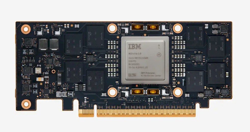
The AIU device that IBM Research has revealed will be based on a 5 nanometer process, and is presumably being fabbed by Samsung, who is IBM’s partner for its 7 nanometer “Cirrus” Power10 processors for enterprise servers and its “Telum” System z16 processors for its mainframes. The Power10 chips have very powerful vector and matrix math units that are an evolution of the designs that have been in use by IBM for many decades, but the Telum chip is using a third generation of IBM Research’s AI Core mixed precision matrix math unit as an on-chip AI inference and low-precision AI training accelerator.
The initial AI Core chip was announced in 2018 and was able to do FP16 half-precision math and FP32 single precision accumulate and was instrumental in IBM’s work to bring even lower precision data and processing to neural networks. After creating the AI accelerator for the Telum z16 processor, which we detailed here back in August 2021, IBM Research took this AI accelerator as a fundamental building block and scaled it up on a single device.
Let’s review the AI accelerator on the Telum chip before getting into the new AIU.
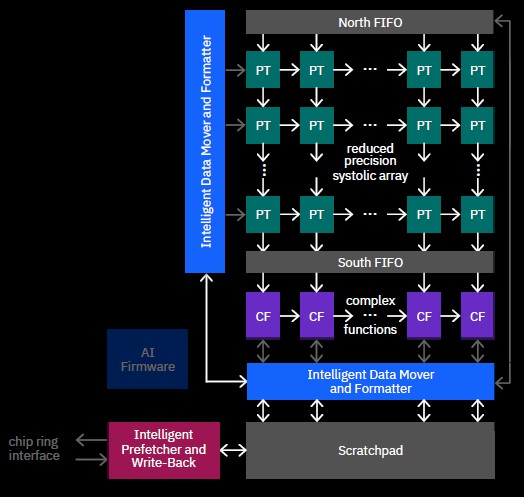
On the z16 chip, the AI accelerator is comprised of 128 processor tiles, probably arranged in a 2D torus configuration that is 4 x 4 x 8 in dimensions — it could be a pair of 4 x 4 x 4 arrays physically and 4 x 4 x 8 logically and looks like that from the die shot — but IBM has not been clear about this. That systolic array supports FP16 matrix math (and its mixed precision variants) on FP32 multiply-accumulate floating point units. This was designed explicitly to support the matrix math and convolutions of machine learning – including not just inference but low precision training, which IBM expects might happen on enterprise platforms. We think it probably also supports the FP8 quarter precision format for AI training and inference as well as INT2 and INT4 for AI inference that we see in this experimental four-core AI Core chip revealed by IBM Research in January 2021 for embedded and mobile devices. The AI Accelerator in the Telum CPU also has 32 complex function (CF) tiles, which support FP16 and FP32 SIMD instructions and are optimized for activation functions and complex operations. The list of special functions supported include:
- LSTM Activation
- GRU Activation
- Fused Matrix Multiply, Bias op
- Fused Matrix Multiply (w/ broadcast)
- Batch Normalization
- Fused Convolution, Bias Add, Relu
- Max Pool 2D
- Average Pool 2D
- Softmax
- Relu
- Tanh
- Sigmoid
- Add
- Subtract
- Multiply
- Divide
- Min
- Max
- Log
A prefetcher and write-back unit hooks into the z16 core and L2 cache ring interconnect, and also links into a scratchpad that in turn links to the AI cores through a data mover and formatting unit, which as the name suggests formats data so it can be run through the matrix math unit to do its inferencing and yield the result. The pre-fetcher can read data out of the scratchpad at more than 120 GB/sec and can store data into the scratchpad at more than 80 GB/sec; the data mover can pull data into and push data from the PT and CF cores in the AI unit at 600 GB/sec.
On the System z16 iron, IBM’s own Snap ML framework and Microsoft Azure’s ONNX framework are supported in production, and Google’s TensorFlow framework has just recently gone into open beta two months ago.
Now, imagine that you copy that AI accelerator off the Telum chip and paste it into a design 34 times, like this:
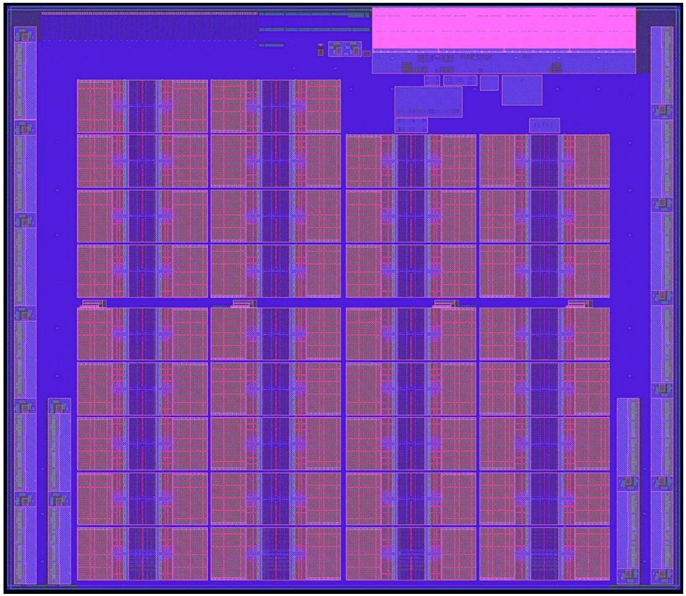
Those 34 cores and their uncore regions for scratchpad memory and linking the cores to each other and the outside system have a total of 23 billion transistors. (IBM says that there are 32 cores on the AIU, but you can clearly see 34, and so we think two of them are there to increase chip yields on devices with 32 usable cores.)
The Telum z16 processors weigh in at 5 GHz, but it is unlikely that the AIU runs at anything near that speed.
If you look at the AIU die, it has sixteen I/O controllers of some sort, which are probably generic SerDes that can be used for memory or I/O (as IBM has done with its OpenCAPI interfaces for I/O and memory in the Power10 chip). There are what appears to be eight banks of LPDDR5 memory from Samsung on the package as well, and that would be 48 GB of memory in total and delivers around 43 GB/sec of aggregate bandwidth. If those are all memory controllers, then the memory could be doubled up to 96 GB/sec and 86 GB/sec of aggregate bandwidth.
The controller complex at the top of the AIU die is probably a PCI-Express 4.0 controller, but hopefully it is a PCI-Express 5.0 controller with support for the CXL protocol built in.
IBM has not said what kind of performance to expect with the AIU, but we can make some guesses. Back in January 2021, a four-core AI Core chip debuted at the ISSCC chip conference, etched by Samsung in 7 nanometers, that delivered 25.6 teraflops of FP8 training and 102.4 teraops in INT4 inference running at 1.6 GHz. This test chip ran at 48.6 watts and had 8 MB of on-chip cache.
This AIU has 34 cores with 32 of them active, so it should have 8X the performance assuming the clock speed remains the same (whatever that was) and 8X the on-chip cache. This would work out to 204.8 teraflops for AI training in FP8 and 819.2 teraops for AI inference with 64 MB of on-chip cache, in something south of a 400 watt power envelope when implemented in 7 nanometers. But IBM is implementing it with Samsung in 5 nanometers, and that probably puts the AIU device at around 275 watts.
By comparison, a 350 watt PCI-Express 5.0 version of the “Hopper” GH100 GPU from Nvidia delivers 2 TB/sec of bandwidth across 80 GB of HBM3 memory and 3.03 petaflops of FP8 AI training performance with sparsity support on.
IBM Research is gonna need AI cores. Lots of AI cores.
Here’s the other issue: Money. If Nvidia is going to charge somewhere north of $20,000 and south of $30,000 for an H100 — and there are indications it will be more north than south — and IBM can put the AIU in the field for $1,000, it can be a spoiler. It might take ten AIUs to match the peak performance of an H100, or five if sparse data is not used, but at 1/20th to 1/30th the cost, watts and space and electricity become secondary things for a lot of organizations. Which is why there were Nvidia P4, T4, and L40 GPU accelerators for AI inference in the first place.