


Intel has the kind of control in the datacenter that only one vendor in the history of data processing has ever enjoyed. That other company is, of course, IBM, and Big Blue wants to take back some of the real estate it lost in the datacenters of the world in the past twenty years.
The Power9 chip, unveiled at the Hot Chips conference this week, is the best chance the company has had to make some share gains against X86 processors since the Power4 chip came out a decade and a half ago and set IBM on the path to dominance in the RISC/Unix market.
IBM laid out a roadmap out past 2020 for its Power family of processors back at the OpenPower Summit in early April, demonstrating its commitment the CPU market with chips that are offer a brawny alternative to CPUs and accelerators compared to the Xeon and Xeon Phi alternatives from Intel and the relatively less brawny chips from ARM server chip makers such as Applied Micro and Cavium and the expected products from AMD, Broadcom, and Qualcomm. We pondered IBM’s prospects in the datacenter in the wake of some details coming out about next year’s Power9 processors, which IBM said at the time would come in two flavors, one aimed at scale-out machines with one or two sockets and another aimed at scale up machines with NUMA architectures and lots of sockets and shared memory.
As it turns out, IBM will be delivering four different variants of the future Power9 chip, as Brian Thompto, senior technical staff member for the Power processor design team at the company, revealed in his presentation at Hot Chips. There was only one Power7 and one Power7+, with variants just having different cores and caches activated. There were three Power8 chips, one with six cores aimed at scale out workloads and with two chips sharing a single package and one single-die, twelve-core chip aimed at bigger NUMA machines; this year saw the launch of the Power8 chip (not a Power8+ even though IBM did call it that for some time) with twelve cores with the NVLink interconnect from Nvidia woven into it.
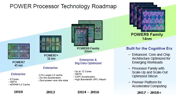
With the Power9 chip, there will be the Power9 SO (short for scale out) variant for machines aimed at servers with one or two sockets, due in the second half of 2017, and the Power9 SU (short for scale up) that will follow in 2018 for machines with four or more sockets and, we think, largely sold by IBM itself for its customers running its own AIX and IBM i operating systems.
The four versions of the Power9 chip differ from each other in terms of the number of cores, whether or not the systems have directly attached memory or use the “Centaur” memory buffer chips, and level of simultaneous multithreading available for specific server configurations, as shown below:
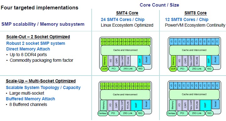
The twist on the SMT level is the new bit we did not know, and we also did not know the core counts that would be available on the Power9 SU variants. We knew that the Power9 SO chip would have 24 cores, and by the way, Thompto tells The Next Platform that the Power9 SO chip is a single die chip with 24 cores. The Power9 SU chip will top out at twelve cores, just like the biggest Power8 chip did. Both Power9 chips have eight DDR memory ports, each with its own controller on the die, which now can either talk directly to two DDR memory sticks on the Power9 SO or to a Centaur buffer chip that in turn talks to four DDR memory sticks each.
Thompto said that the Power9 SO chip has 120 GB/sec of sustained memory bandwidth with lower latency than was possible with the buffered memory setup with the Power8 and with the Power9 SU coming out in 2018. The Power9 SO chip aimed at the commodity two-socket server space where Intel’s Xeon E5 chips rule can use the same commodity DDR4 memory sticks, and the Power9 SO will come in a commodity form factor packaging that is more like the Xeon E5 than the current Power8. Architecturally, Thompto says that the Power9 SO can support a maximum of 4 TB of main memory using 256 GB memory sticks, but practically speaking, using 64 GB memory sticks the capacity will top out at 1 TB for these systems.
The Power9 SU machines, on the other hand, will have eight buffered channels and have up to 8 TB of main memory available across the 32 memory slots each socket can support, provided customers can afford 256 GB sticks. Again, 2 TB per socket is the practical, economic limit for memory for most customers. That buffered memory also implements an L4 cache on the Centaur chip, and also implements chip kill and lane sparing, and will be compatible with existing Power8 memory cards, which is something Big Blue’s existing Power Systems customers will like to hear. The extra RAS features and the 230 GB/sec of sustained memory bandwidth per socket is also a key differentiator for the Power8 and Power9 SU chips, and something that IBM no doubt wishes it were possible to bring down to the Power9 SO. But that would have necessitated putting sixteen DDR4 ports on the Power9 SU chip for a total of 32 memory sockets, and for whatever reason, IBM did not do this.
In addition to the different core counts and memory options, IBM is making the Power9 SO and Power9 SU chips available with two different levels of simultaneous multithreading, SMT4 with up to four virtual threads per core and SMT8 with up to eight virtual threads per core. IBM already supports SMT8 with the Power8 chips, and backstepping to SMT4 for versions of the chips may seem like an odd choice. But according to Thompto, the Power9 SMT4 chips are designed with a focus on Linux systems that want high core counts and that want to have the most granularity for server virtualization, while the Power9 SMT8 chips are optimized for large logical partitions with IBM’s PowerVM hypervisor and for workloads that need more threads rather than stronger threads.
This would suggest that the SU chips will have fewer cores and higher clocks, as we suspected back in April, while the SO chips will have more cores but lower SMT levels and presumably lower clocks. But, just for fun, there is an SU chip that will have 24 cores and the SO chip will be available in a twelve-core variant, too, just in case there are workloads that will go in different directions.
Drilling Into The Core
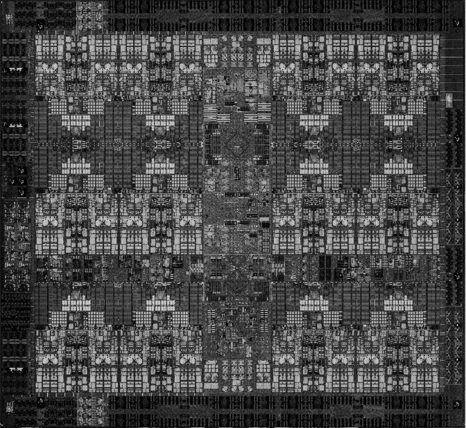
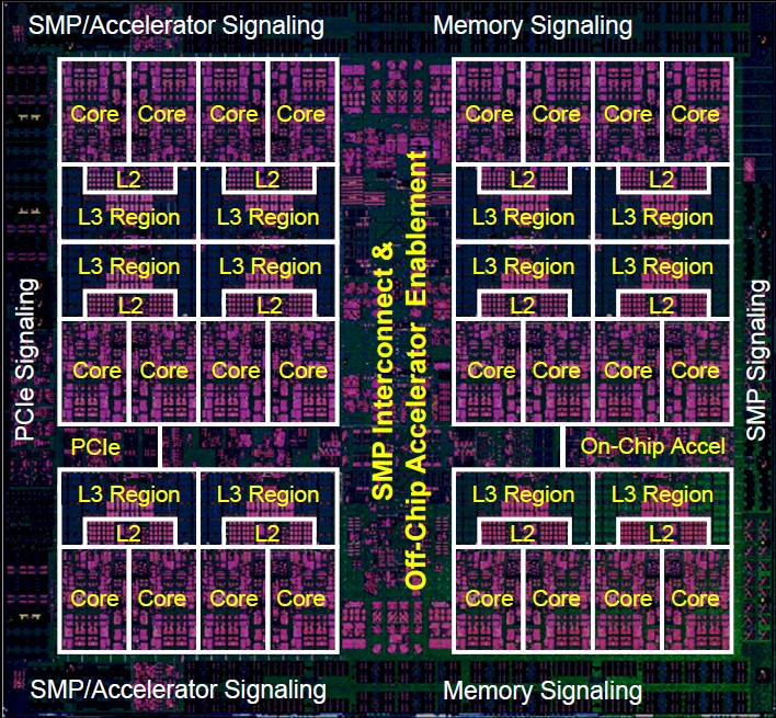
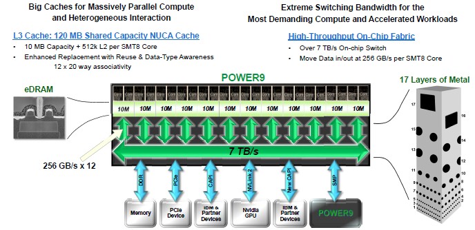
The Power9 chip is a biggie, weighing in at 8 billion transistors. It is made using the 14 nanometer FinFET manufacturing processes from Globalfoundries, which acquired IBM’s fab business two years ago (the 14HP process, to be specific). This process has 17 layers and significantly makes use of the embedded DRAM (eDRAM) memory perfected by Big Blue in the Power7, Power7+, and Power8 chips to create a 120 MB shared L3 cache for all of the cores on the Power9 SO die.
Here is what the Power9 SO die looks like:
And here is what it looks like when you block off its main components:
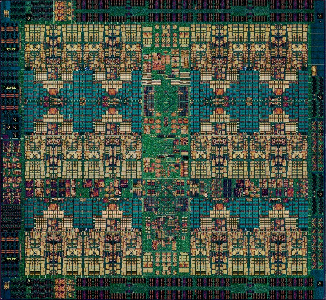
IBM did not provide a die shot or block diagram of the twelve core variants of the Power9 SU and Power9 SO chips, but they don’t really have that much of a different size and layout for the transistors because of the way the fat SMT8 and skinny SMT4 cores have been created using what IBM calls an execution slice microarchitecture.
“We started with a 64 bit compute building block and we coupled that with a 64 bit load store building block,” explained Thompto. “Each compute building block has a heterogeneous mix of compute, fixed and float, supporting scalar and vector. This allows us to obtain high utilization of our compute resources while also providing seamless exchange of data and shared data paths. It also serves as an efficient building block for managing instruction flow through the machine. We couple two of these 64 bit slices together to make a 128 bit superslice, and this is our physical design building block.”
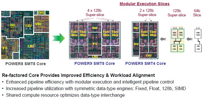
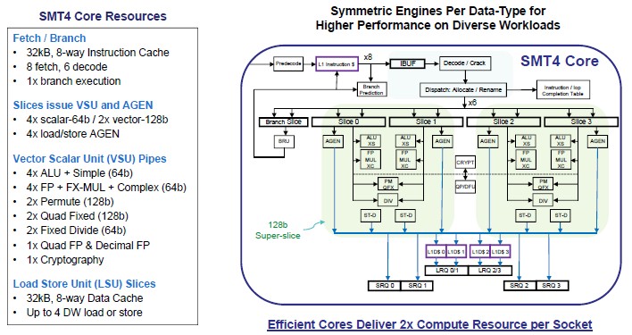
Two of these superslices comprise an SMT4 core, and four of them comprise an SMT8 core, and Thompto says that the Power9 pipeline was shorter from fetch to compute by five cycles compared to the Power8 core and had better branch prediction. The SMT4 core can do 64 instructions per cycle and the SMT8 core can do twice that at 128 instructions per cycle. The end result of all of the tweaks in the microarchitecture is a leaner and stronger core. Here are the feeds and speeds of the Power9 SMT4 core:
The Power9 chip is the first chip from IBM to support the Power 3.0 instruction set, which has a number of tweaks to it. First of all, the new ISA definition supports 128-bit quad-precision floating point math that is compliant with the IEEE 754 standard and, importantly, is useful for certain financial services and security applications that require higher precision floating point math. The new ISA also supports 128 bit decimal integer math, which is useful with databases and anything that is doing money math. IBM has also added a single-instruction random number generator, which is important for all kinds of simulations that require lots of randomness (it took more than one cycle to do this with the Power8 chips). There are a slew of other nips and tucks, including hardware assisted garbage collection for Java, PHP, and other interpreted languages and a new interrupt architecture that will make highly virtualized environments (presumably both OpenKVM and PowerVM hypervisors) run more smoothly.
The Power9 chip with the SMT8 cores are aimed at analytics workloads that are wrestling with lots of data, in terms of both capacity and throughput. The 24 core variant of the Power9 with SMT8 has 512 KB L2 cache memory per core, and 120 MB of L3 cache is shared across the dies in 10 MB segments with each pair of cores. The on-chip switch fabric can move data in and out of the L3 cache at 256 GB/sec, and adding in the various interconnects for memory controllers, PCI-Express 4.0 controllers, and the “Bluelink” 25 Gb/sec ports that are used to attach accelerators to the processors as well as underpinning the NVLink 2.0 protocol that will be added to next year’s “Volta” GV100 GPUs from Nvidia and IBM’s own remote SMP links for creating NUMA clusters with more than four sockets, and you have an on-chip fabric with over 7 TB/sec of aggregate bandwidth.
The Power9 chips will have 48 lanes of PCI-Express 4.0 peripheral I/O per socket, for an aggregate of 192 GB/sec of duplex bandwidth. In addition to this, the chip will support 48 lanes of 25 Gb/sec Bluelink bandwidth for other connectivity, with an aggregate bandwidth of 300 GB/sec. On the Power9 SU chips, 48 of the 25 Gb/sec lanes will be used for remote SMP links between quad-socket nodes to make a 16-socket machine, and the remaining 48 lanes of PCI-Express 4.0 will be used for PCI-Express peripherals and CAPI 2.0 accelerators. The Power9 chip has integrated 16 Gb/sec SMP links for gluelessly making the four-socket modules. In addition to the CAPI 2.0 coherent links running atop PCI-Express 4.0, there is a further enhanced CAPI protocol that runs atop the 25 Gb/sec Bluelink ports that is much more streamlined and we think is akin to something like NVM-Express for flash running over PCI-Express in that it eliminates a lot of protocol overhead from the PCI-Express bus. But that is just a hunch. It doesn’t look like the big bad boxes will be able to support this new CAPI or NVLink ports, by the way, since the Bluelink ports are eaten by NUMA expansion.
The bandwidth improvement with this new CAPI and NVLink 2.0 running atop Bluelink is impressive. Moving from a PCI-Express 3.0 x16 slot to one using PCI-Express 4.0 doubles up the peak bandwidth, says Thompto, and adding NVLink to the Power8 chip with four ganged up NVLink 1.0 ports boosted the bandwidth between the processor and a “Pascal” Tesla P100 GPU by 5X. With the Bluelink ports, the bandwidth between the Power9 chip and accelerators will be anywhere from 7X to 10X higher, depending on the accelerator and the protocol.
So how will the Power9 chip perform? It depends on the workload. Take a look:

In the comparison above, IBM is comparing a Power8 chip with twelve cores using SMT8 threading running at 4 GHz to a Power9 chip with the same clock speed, core count, and threading. In this case, performance increases range from a low of around 50 percent to a high of 125 percent. It will be interesting to see how the different clock speeds, thermals, SMT levels, and memory bandwidth all add up to different performance across the Power9 line and compared to Xeon, Opteron, and ARM alternatives coming to market next year.
2017 is gonna be a lot of fun for server processors. That much we know for sure. We will be drilling down into the system options for the Power9 chips in a follow-on story.