


At AMD’s Epyc launch few weeks ago, Lisa Su, Mark Papermaster, and the rest of the AMD Epyc team hammered home that AMD designed its new Zen processor core for servers first. This server-first approach has implications for performance, performance per watt, and cost perspectives in both datacenter and consumer markets.
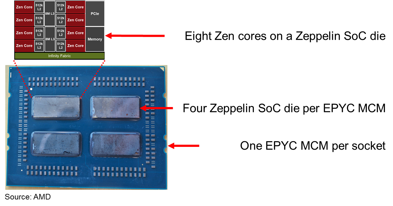
AMD designed Epyc as a modular architecture around its “Zeppelin” processor die with its eight “Zen” architecture cores. To allow multi-die scalability, AMD first reworked its HyperTransport socket-to-socket system I/O architecture for use on a chip, across a multi-chip module (MCM), and for inter-socket connectivity. AMD has named this coherent connection the Infinity Fabric.
There are several benefits of this design from which AMD benefits. Epyc uses Infinity Fabric and the modular Zeppelin die design to fundamentally change:
- The economics for designing large die area, large core count server system-on-chip (SoC) and MCM products
- Memory and I/O scalability within a socket
- The concept of socket availability and reliability over time
- The economics of designing for the commercial markets first, but using the same components for consumer markets via a different back-end production flow
- The economics of single-socket (1S) servers
AMD’s Epyc launch also showed more breadth and depth for customer support and ecosystem development than we have seen at any other AMD launch this millennium.
Infinity Fabric
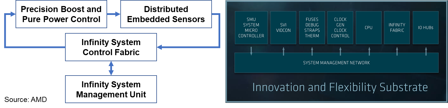
Starting with AMD’s Ryzen desktop processor and Epyc server architecture, AMD will implement their scalable Infinity Fabric across all its SoC and MCM products. Think of Infinity Fabric as a superset of HyperTransport, AMD’s previous socket-to-socket interconnect architecture, now managed by the HyperTransport Consortium. Infinity Fabric is a coherent high-performance fabric that uses sensors embedded in each die to scale control and data flow from die to socket to board-level.
AMD redesigned HyperTransport as a software-defined interconnect fabric, and as such Infinity Fabric has separate and scalable control and data paths. In software defined networking (SDN), these paths are referred to as planes – control planes and data planes, to be specific – and the architectural implementation is similar.
Infinity Fabric’s System Control Fabric (SCF) uses on-die embedded sensors to monitor die temperature, speed, and voltage 1,000 times per second across all 64 cores within the eight Zeppelin dies that are crammed into a dual-socket system. SCF and Epyc’s system management unit work together in real-time to identify optimal operating settings. SCF uses fine-grained frequency control in 25 MHz clock speed increments, and it also enables operators to customize the balance of performance and power consumption for specific workloads or use cases. Infinity Fabric also controls power management, security, reset and initialization, and die test functions. If fewer cores are enabled, then frequency boost is automatically enabled within temperature and current delivery limits.
Customers can order Epyc processors pre-configured for:
- Consistent performance across all normal real-time variations of datacenter cooling and power delivery
- Maximum performance at a fixed power consumption, where performance may vary depending on real-time cooling efficiencies
Infinity Fabric’s System Data Fabric (SDF) connects the L3 caches to memory and to the configurable I/O lanes (described below). SDF uses the configurable I/O lanes for memory coherent communications between compute elements on a single die, between different dies mounted on an MCM, and between sockets in a NUMA server design. Using Infinity Fabric, AMD can connect multiple dies on a printed circuit board and enable the MCM to act as a single monolithic compute node.

The figure above shows how AMD describes Infinity Fabric scaling:
- SCF connects compute elements
- SDF enables coherent communications among caches and between caches and memory. There are four fully interconnected core complexes on a Zeppelin die (see below for much more detail on Zeppelin). Each Infinity Fabric on-die link is four-bit point to point.
- Both SCF and SDF scale between die on an MCM and between sockets
AMD tuned a specific implementation of Infinity Fabric for two-socket servers. Future multi-socket Infinity Fabric implementations do not have to implement this specific topology, as it has a high lane count to maximize cross-sectional bandwidth. AMD’s goal was to match the cross-sectional bandwidth within each MCM with the cross-sectional bandwidth of the links between the MCMs.
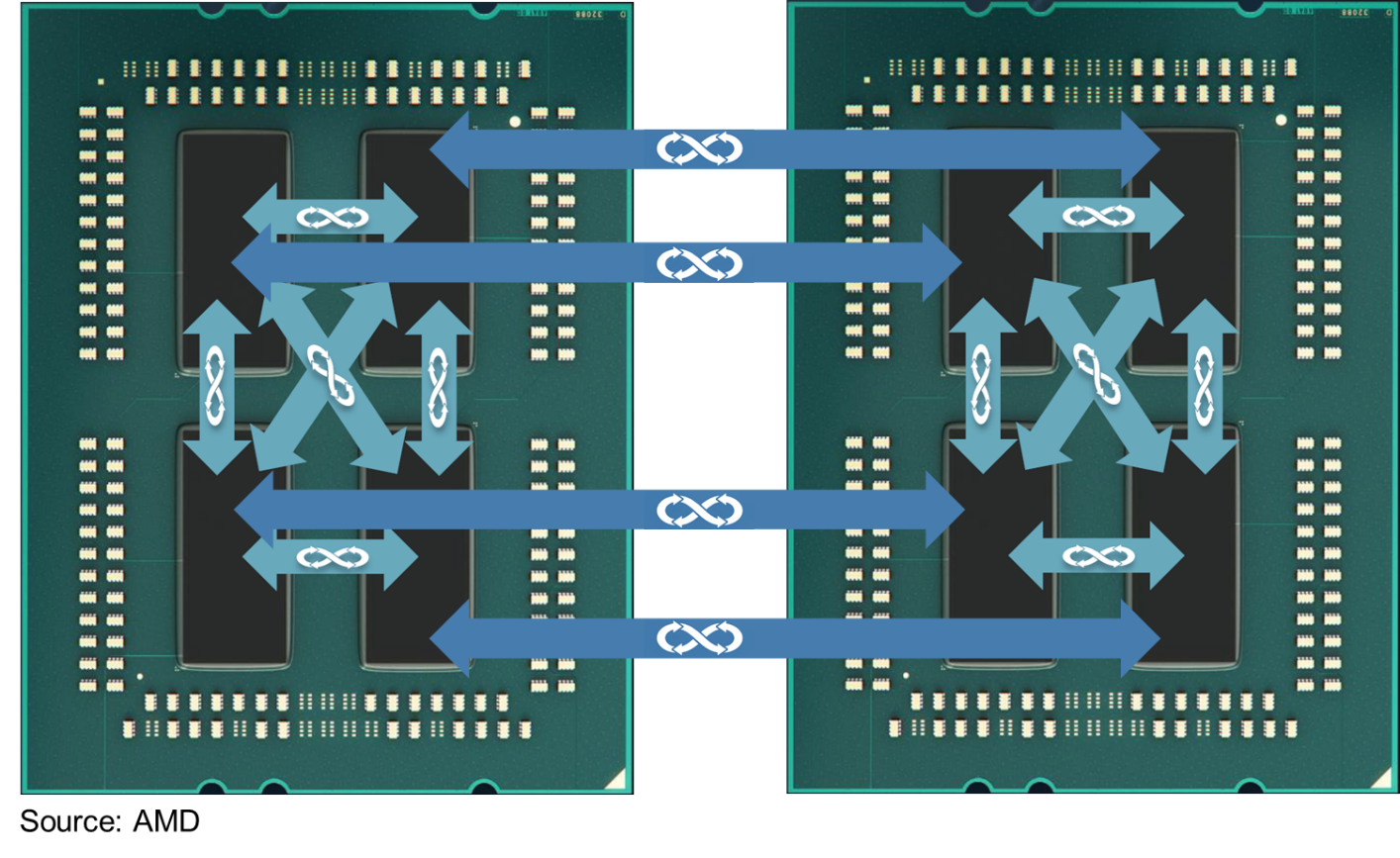
The figure above shows another rendition of a fully connected MCM highlighting that Infinity Fabric directly connects a die on one MCM to its matching die on the other MCM. This creates a sparsely connected hypercube where memory attached to one die is at most only two “hops” (intermediary memory controllers attach to the SDF, the memory controllers are in different die) away from any part of system memory. This interconnect topology is analogous to the eight-socket Opteron servers built with HyperTransport a dozen years ago as we pointed out in our original coverage of Epyc back in June, but now it is collapsed into a higher-performance two-socket design.
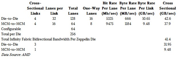
Each Infinity Fabric link between two Zeppelin dies on an MCM is 32-lanes wide, supporting full-speed operation on 16 lanes in each direction. We calculate that AMD is running these links at an unaggressive speed of 5.3 Gb/sec to conserve power and make MCM PCB design easier, for an aggregate throughput of 10.65 GB/sec point-to-point between chips (see Table 1 below for more detail). AMD measures the cross-sectional bandwidth of Infinity Fabric across the Epyc MCM as four times that, or 42.6 GB/sec, but we think the more important metric is the 41.4 GB/sec aggregate bandwidth of the Infinity Fabric links on each die in a two-socket system.
Each of the four Infinity Fabric connections between the two sockets uses the same serializer-deserializer (SERDES) links used by the 16 PCI-Express 3.0 lanes, but operating 20 percent faster than the PCI-Express 3.0 link, at about 9.5 Gb/sec each for 9.5 GB/sec bidirectional bandwidth between processors and an aggregate cross section of 37.9 GB/sec bidirectional bandwidth between sockets.
As a cross check, we calculate there are 256 dedicated Infinity Fabric and configurable I/O lanes available (ignoring the memory controllers and the uncore external I/O) on each Zeppelin die. (“Uncore” describes functions on a die that do not directly contribute to the compute and memory subsystems.) That seems like a great answer from a digital design point of view, as 2 to the 8th is one of our magic numbers.
Infinity Fabric also implements a scalable Machine Check Architecture (MCA). The control fabric reports MCA errors at the die and the link level. If a failure occurs, the MCA can implement data poisoning and other reliability assurance measures. For example, as long as the die-to-die links and memory are still operating correctly, it becomes a run-time operating system policy decision to ignore a core that has become unreliable (has exceeded a threshold for deferred or correctable errors) and allow the rest of the cores in a Epyc MCM to remain operational.
MCM Interconnect Competition
Epyc’s multi-die design and MCA architecture are fundamentally different than Intel’s monolithic Xeon architecture. The Zeppelin die’s embedded error reporting and management combines with the Infinity Fabric architecture’s ability to understand that a cluster of Zeppelin dies in a MCM defines a single management and service domain.
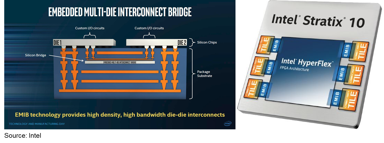
Intel’s Embedded Multi-die Interconnect Bridge (EMIB), by comparison, appears to be a simple point-to-point physical communications link between two die, using only a physical layer protocol. I have seen no mention of higher-leveler protocols in any of Intel’s EMIB public disclosures. Intel states that EMIB can be used to decouple I/O transceivers from compute logic (because they may each perform better when manufactured in different silicon processes) or in a more general sense as a high-speed interconnect for any two die mounted on the same multi-chip package substrate.
EMIB embeds a separate bridge die into the underlying package substrate, as well as transceiver logic in each of the two die connected by the bridge. A bridge chip sits under the two die it connects (see the figure below). This seems much more complex (which implies that it is more expensive) than AMD’s approach of using standard PCBs as the planar for MCMs.
Intel has only shipped EMIB in its Stratix 10 FPGA, where EMIB is used solely to connect FPGA silicon with “connectivity tiles” to provide high-speed I/O off of the FPGA die. Intel has not shipped EMIB for the general case of connecting multiple compute die, yet. TIRIAS Research predicts that Intel will continue to espouse a perceived value for large, expensive, monolithic compute die until they introduce a multi-die compute product based on EMIB or subsequent die interconnect technologies.
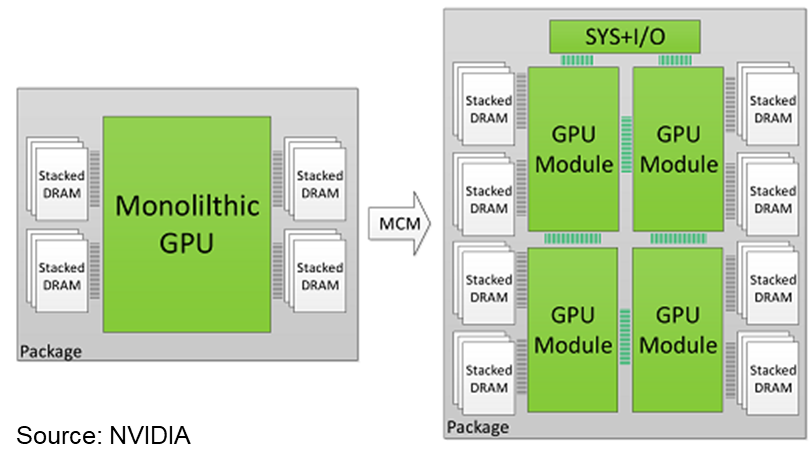
Nvidia has also been experimenting with MCMs. Its Volta generation V100 GPU die measures a reticle-filling 815 millimeters square in TSMC’s 12 nanometer process; this is likely to remain the largest production die ever shipped. Having reached the practical limits of a monolithic die, Nvidia recently published a research paper (see the figure below) that proposes three features for a future multi-chip GPU architecture:
- Create an “L1.5” cache as an extension of the L1 cache that captures remote memory changes in a local cache on each GPU die
- Use distributed scheduling for co-operative thread arrays (CTA) instead of a global scheduler, used in monolithic GPUs
- Optimize DRAM memory page allocation to minimize memory traffic between GPU die using a “first touch” page mapping policy that maps a memory page into the local memory partition of the first GPU die to request the page
Like AMD, Nvidia’s paper recommends using “a low-effort, low-cost, and low-energy link design point,” in this case 768 GB/sec, and notes that architectural innovation can improve communications, mitigating the need for more expensive and power-hungry links. It looks like Nvidia is siding with AMD in this architectural debate.
Lastly, because of Infinity Fabric, Epyc looks like a monolithic processor from a software development point of view – middleware and application developers do not need to do anything different than their standard performance tuning and instruction set optimizations. The operating system, hypervisor, container, and management framework developers also do not need to do anything differently, either, but they might choose to work with AMD to customize management and routing behaviors to their specific needs. For example, different system vendors might specify different behaviors to respond to a memory channel failure or a failed link between die. Infinity Fabric and Epyc provide a unique capability for resilience tuning.
In the second part of this article, we will expand out into the system designs that use the Epyc processors, which are ultimately what matters to server makers and buyers.
Paul Teich is an incorrigible technologist and a principal analyst at TIRIAS Research, covering clouds, data analysis, the Internet of Things and at-scale user experience. He is also a contributor to Forbes/Tech. Teich was previously CTO and senior analyst for Moor Insights & Strategy. For three decade, Teich immersed himself in IT design, development and marketing, including two decades at AMD in product marketing and management roles, finishing as a Marketing Fellow. Paul holds 12 US patents and earned a BSCS from Texas A&M and an MS in Technology Commercialization from the University of Texas McCombs School.