


It was only just last month that we spoke with Google distinguished hardware engineer, Norman Jouppi, in depth about the tensor processing unit used internally at the search giant to accelerate deep learning inference, but that device—that first TPU—is already appearing rather out of fashion.
This morning at the Google’s I/O event, the company stole Nvidia’s recent Volta GPU thunder by releasing details about its second-generation tensor processing unit (TPU), which will manage both training and inference in a rather staggering 180 teraflops system board, complete with custom network to lash several together into “TPU pods” that can deliver Top 500-class supercomputing might at up to 11.5 petaflops of peak performance.
“We have a talented ASIC design tea that worked on the first generation TPU and many of the same people were involved in this. The second generation is more of a design of an entire system versus the first, which was a smaller thing because we were just running inference on a single chip. The training process is much more demanding, we need to think holistically about not just the underlying devices, but how they are connected into larger systems like the Pods,” Dean explains.
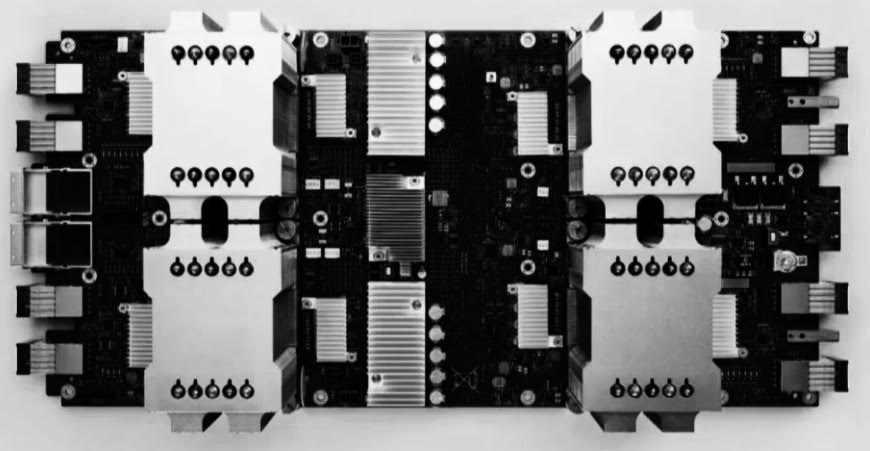
We will follow up with Google to understand this custom network architecture but below is what were able to glean from the first high-level pre-briefs offered on the newest TPU and how it racks and stacks to get that supercomputer-class performance. Google did not provide the specifications of the TPU2 chip or its motherboard, but here is the only image out there that we can start doing some backwards math with.
To our eyes it looks a little like a Cray XT or XC boards, which we find amusing, except that the interconnect chips seem to be soldered onto the center of the motherboard and the ports to the outside world are on the outside of the board. This TPU2 board has four of the TPU2 units, each board capable of a maximum peak throughput of 45 teraflops with the system board having an aggregate of 180 teraflops as we have said above. (We presume that this is using 16-bit half-precision floating point.)
There are eight interconnect ports on the left and right edges, plus another two ports on the left hand edge that break the pattern. It would be interesting if each TPU2 board had direct access to flash storage, as AMD is doing with its future “Vega” Radeon Instinct GPU accelerators. Those two ports on the left could be for linking directly to storage, or they could be an uplink to a higher level in the network used to interconnect the TPUs into a processing complex.
If we had to guess – and we do until Google divulges more details – each TPU2 has two ports to the outside world and across the racks and the two extra ports on the left are for local storage and for node interconnect within the rack. (Google could be implementing a loosely coupled or somewhat tight memory sharing protocol across these interconnects if they are fast enough and fat enough, and that would be neat.)
Here is what a pod of the TPU2 boards looks like, which Google says has an aggregate of 11.5 petaflops of machine learning number crunching capacity:
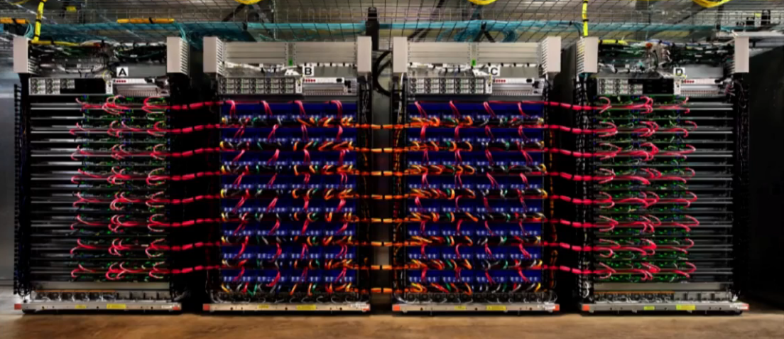
Take a hard look at it. From our eyes, it looks like these are actually Open Compute racks, or something about the same dimensions if not a little wider. There are eight rows of TPU units, with four of the TPU boards per enclosure horizontally. We can’t tell if the rack is full depth of half depth. You can see the six ported sides are poking out of the racks of TPU2 compute nodes, and those two ports reach up into enclosures above them.
Above the top row of TPU2 enclosures, those two ports reach up into an enclosure that does not appear to have TPU2 units in them. Our guess is that this is a bare bones flash enclosure that stores local data at high speed for the TPUs. In any event, we can see this has at least 32 of the TPU2 motherboards, which means it has 128 TPUs in the rack. If we do the math on that, this works out to the 11.5 petaflops across those two racks with the blue covers, which make up the pod.
For perspective on what all this floating point goodness means on the production end, Google’s newest large-scale translation model takes an entire day to train on 32 of the “best commercially available GPUs” (we can assume Pascal)—while one 1/8 of a TPU pod can do the job in an afternoon. Keep in mind, of course, that the TPU is tailor-made for chewing on TensorFlow while commercial GPUs, even those at the highest end, have to be general purpose enough to suit both high- and low-precision workloads. Still, the ROI of Google rolling its own ASIC are not difficult to wrangle from this example.
As an additional point, remember that with the first generation TPU, Google might have had super-fast and efficient inference, but that model had to be moved from a GPU training cluster first, which slows experimentation with new or retrained models moving into deployment and made developers at Google have to wait longer for results before iterating on their work. It is for this reason that the training/inference on a single device is the holy grail of deep learning hardware–and we are finally at a point where there are multiple options cropping up for just that; in the future, Knights Mill from Intel, but of course–and freshest in our minds–is the Volta GPU.
Nvidia’s Volta GPUs, with “tensor core” processing elements for speeding machine learning training as well as eventual supercomputing workloads, can achieve 120 teraflops on a single device, a major advantage from Pascal, just released a year ago. While that cadence is impressive, Google’s announcement just stole some of the oxygen from Nvidia’s announcement—even if users will never get their hands on their own in-house TPU-powered machine anytime soon.
Dean says that the Volta architecture is interesting in that Nvidia realized “the core matrix multiply primitive is important to accelerating these applications.” He adds that Google’s first generation TPU also took the same idea of speeding matrix multiplication for inference, but of course, this device is doing that across the machine learning workflow. “Speeding up linear algebra is always a good idea,” he notes.
Hardware aside for a moment, here’s the really interesting bit from a user perspective. Instead of keeping its secret sauce inside, Google will be making these TPUs available via the Google Cloud Platform in the near future. The company’s senior fellow, Jeff Dean, says that they do not wish to limit competition and will be offering the TPU as an option, along with Volta GPUs and continuing with Skylake Xeons (which GCP already has), Dean says, as well to give developers several options about how to build and execute their models. Google will also be offering 1000 TPUs in its cloud for qualified research teams that are working on open science projects and might be willing to open source their machine learning work.
Dean explains that while GPUs and CPUs will still be used for some select internal machine learning workloads inside Google, the power of having both training and inference on the same device—one that is tuned for TensorFlow will change the balance. While the power specs of the newest TPU were not relayed, we should note that the skinny power consumption of the first-generation device is not a good yardstick for gauging efficiency of the new device since it is doing both training and inference. We can speculate that the power consumption is lower than Volta, which is a massive device by any measure, but that also is being tasked with supporting a wide range of workloads, from some HPC applications that will require 64-bit floating point, all the way down to ultra-low precision workloads in machine learning. Nvidia standardized its approach on FP16 so users could cobble together or pare their precision according to workload, but we have to assume this newest TPU architecture is geared toward 16- or 8-bit. We hope to verify in a follow-up with lead engineers.
On that note, Dean did say that “Unlike the first generation that supported quantized integer arithmetic, this uses floating point computations. You won’t have to transform the model once its trained for inference to use quantized arithmetic, you can use the same floating point representation throughout training and inference, which will make this easier to deploy.”
It is a good thing for Nvidia and Intel that Google is not in the business of pushing its custom-developed hardware into the market, because the TPU is woefully competitive in a market where both seek an edge. Putting the second-generation TPU in the Google Cloud Platform will certainly send some users that way for large-scale training, but as noted, there will also be high-end GPUs as well as CPUs for those workloads. The ability for users to use TensorFlow at scale on an architecture designed just for that purpose will be compelling however. We imagine that this move will light a fire under Amazon and Microsoft with its Azure cloud to step to when it comes to offering latest-generation GPUs, something they have been slow about doing (the highest-end GPU available on Amazon is the Tesla K80, but Pascal P100s are now available on Azure).
For those who keep wondering why Google doesn’t commercialize its chips, read above and see how Google is already doing this–albeit via a less direct route (and one with less risk, for that matter). If indeed these deep learning markets expand at the level predicted, the differentiation provided by TPU and TensorFlow will be enough to give Google Cloud Platform an edge like it’s never had before. That gets them around mass production–and into a mass user base, and one that can help it build out TensorFlow in the process.
As a side note, we have to harken back to Google’s motto from so many years ago… “Don’t be evil.” Because let’s be honest, going public with this beast during the Volta unveil would have been…yes, evil.