


Graphics chip maker Nvidia has taken more than a year and carefully and methodically transformed its GPUs into the compute engines for modern HPC, machine learning, and database workloads. To do so has meant staying on the cutting edge of many technologies, and with the much-anticipated but not very long-awaited “Volta” GP100 GPUs, the company is once again skating on the bleeding edge of several different technologies.
This aggressive strategy allows Nvidia to push the performance envelope on GPUs and therefore maintain its lead over CPUs for the parallel workloads it is targeting while at the same time setting up its gaming and professional graphics businesses for a significant performance boost – and a requisite revenue jump if history is any guide – in 2018.
The premise with general purpose GPU computing, way back in 2006 when it got started and in 2008 when the Tesla products and the CUDA parallel programming environment debuted in the HPC space that was in dire need of larger increases in application performance at lower costs and thermals than CPUs alone could deliver, was that all of the innovation in gaming and professional graphics would engender a GPU compute business that benefitted from Nvidia’s investments in these areas. Now, to our eye, it looks like the diverse compute needs in the datacenter are driving Nvidia’s chip designs and roadmaps, and for good reason.
The very profitable portion of its business that is embodied in the Tesla and GRID product lines and that are used to accelerate simulation, modeling, machine learning, databases, and virtual desktops has been nearly tripling in recent quarters and shows no signs of slowing down. The datacenter tail has started wagging the gaming dog. And as far as we are concerned, this is how it should be. We believe fervently in the trickle down of technology from high end to enterprise to consumer because the high end has the budget to pay for the most aggressive innovation.
Volta is, without question, the most advanced processor that Nvidia has ever put into the field, and it is hard to imagine what it will be able to do for an encore. That is probably why Nvidia co-founder and chief executive officer, Jen-Hsun Huang, did not talk about Tesla GPU roadmaps during his keynote at the GPU Technology Conference in the company’s hometown of San Jose today during his keynote address.
Back in the earlier part of the decade, as GPU compute moved from academia to the national HPC labs, Nvidia had to prove it had the technical chops to deliver enterprise-grade engines in a timely fashion and without technical glitches. There were some issues with the “Maxwell” line of GPUs in that we never did see a part with lots of double precision flops, and some features slated for one generation of GPU were pushed out to later ones, but Nvidia has more or less delivered what it said it would, and did so on time. This, in and of itself, is a feat and it is why we are not hearing about successors to Volta as this new generation of GPUs is making its debut in the company’s datacenter products.
We don’t expect to hear much about roadmaps until this time next year, in fact, when the Volta rollout will be complete and customers will be wondering what Nvidia will do next.
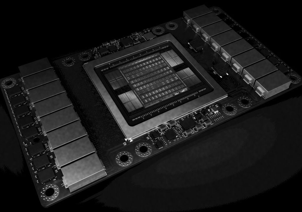
Shockingly Large Volta GPUs
The Volta GV100 chip needed to incorporate a lot more compute, and a new TensorCore matrix math unit specifically designed for machine learning workloads in addition to the floating point and integer units that were in the Pascal GP100 chip that made its debut last April at the GTC shindig. The full Pascal GP100 chip had 56 streaming multiprocessors, or SMs, and a total of 3,584 32-bit cores and 1,792 64-bit cores; with caches, registers, memory controllers, and NVLink interconnect ports, this Pascal GP100 chip weighed in at 15.3 billion transistors using the 16 nanometer FinFET process from Taiwan Semiconductor Manufacturing Corp.
The Volta GV100 chip has 84 SMs, each with 5,376 32-bit floating point cores, 5,376 32-bit integer cores, 2,688 64-bit floating point cores, and 672 TensorCores for deep learning; this chip is implemented in the very cutting edge 12 nanometer FinFET node from TSMC, which is one of the ways that Nvidia has been able to bump up the transistor count to a whopping 21.1 billion for this chip. To help increase yields, Nvidia is only selling Tesla V100 accelerator cards that have 80 or the 84 SMs on the GV100 chip activated, but in time, as yields improve with the 12 nanometer process, we expect for the full complement of SMs to be activated and the Volta chips to get a slight performance boost further from it. If you extrapolate, there is another 5 percent performance boost in there, and more if the clock speed can be inched up a bit.
In any event, the Volta GV100 chip has a die size of 815 square millimeters, which is 33.1 percent larger than the 610 square millimeters of the Pascal GP100 die, and that is about as big as any chip dare to be on a 300 millimeter wafer in such a new manufacturing process.
We will be drilling down into the architecture of the Volta GPUs and the possibilities of the updated NVLink 2.0 interconnect in future stories, but for now, here is the overview of the Volta GV100 GPU. With those 80 SMs fired up on the die and running at 1,455 MHz (1.7 percent slower than the Pascal GP100 clocks), the GV100 delivers 15 teraflops of floating point performance at 32-bit single precision, 7.5 teraflops at 64-bit double precision, which is a 41.5 percent boost in raw computing oomph that is applicable to traditional HPC workloads and to some AI workloads. But here is the interesting bit, those Tensor Core units added to the Volta architecture deliver 120 teraflops of effective performance for machine learning training and inference workloads. To be precise, the Tensor Core units on the Volta GV100 deliver 12X the peak performance of the Pascal GP100 using FP32 units for training and 6X its performance on machine learning inference using FP16 half-precision instructions on the FP32 units. (There was no comparison of inference workloads using the Pascal’s 8-bit integer units compared to Volta’s Tensor Core’s, but logically, it should be somewhere around 3X higher on the Tensor Core units.) All of this within the same 300 watt thermal envelope that its predecessor had.
The Volta GV100 chip has 6 MB of L2 cache, a 50 percent increase over the Pascal GP100 and consistent with the increase in the number of cores. The GV100 has a tweaked set of memory controllers and the Tesla Volta V100 accelerator has 16 GB of an improved variant of HBM2 stacked memory from Samsung. The Pascal P100 card delivered 724 GB/sec of peak memory bandwidth and the Volta V100 card can push 900 GB/sec. This is an order of magnitude higher than a typical two-socket X86 server can do, which is one reason why GPU accelerators are being deployed in HPC workloads. But HPC workloads are largely bound by memory capacity and memory bandwidth, and HPC centers were probably hoping to get GPU accelerators with 24 GB or even 32 GB of capacity and well over 1 TB/sec of bandwidth. There is a lot more compute with Volta, but no more memory capacity and only 24.3 percent more peak memory bandwidth. That said, Nvidia says the new Volta memory architecture actually delivers 1.5X better sustained memory bandwidth than Pascal, and this matters, too.