


Google created quite a stir when it released architectural details and performance metrics for its homegrown Tensor Processing Unit (TPU) accelerator for machine learning algorithms last week. But as we (and many of you reading) pointed out, comparing the TPU to earlier “Kepler” generation GPUs from Nvidia was not exactly a fair comparison. Nvidia has done much in the “Maxwell” and “Pascal” GPU generations specifically to boost machine learning performance.
To set the record straight, Nvidia took some time and ran some benchmarks of its own to put the performance of its latest Pascal accelerators, particularly the ones it aims at machine learning, into perspective, and it shows that the GPU can hold its own against Google’s TPU when it comes to machine learning inference with the added benefit of also being useful for the training of the neural networks that underlie machine learning frameworks. The additional benchmarks also illustrate how hard – and perhaps risky – it is is to make a decision to build a custom chip for machine learning when GPUs are on an annual cadence to boost the oomph. Google made a decision at a point in time to do a better job on machine learning inference, and not coincidentally, so did Nvidia.
As we explained in our coverage on Google’s TPU architecture and its performance results, there is no question that the TPU is a much better accelerator supporting Google’s TensorFlow framework for machine learning when used to run inferencing – which means taking the trained neural network and pushing new data through it in a running application – compared to a single 18-core “Haswell” Xeon E5-2699 v3 processor running at 2.3 GHz or a single Kepler GK210B GPU with 2,496 cores running at their baseline 560 MHz. While the Haswell can support 8-bit integer operations, which is what the TPU uses for inferencing, as well as 64-bit double precision and 32-bit single precision floating point (which can also be used for neural nets but which have diminished performance on machine learning training and inferencing), the higher bitness of the Haswell Xeon did not have a very high throughput in integer mode and could not match the batch size or throughput of the TPU in floating point mode. And a single Kepler GK210B GPU chip, which did not have 8-bit integer support at all and only 32-bit and 64-bit floating point modes, was similarly limited in throughput, as this summary table showed:
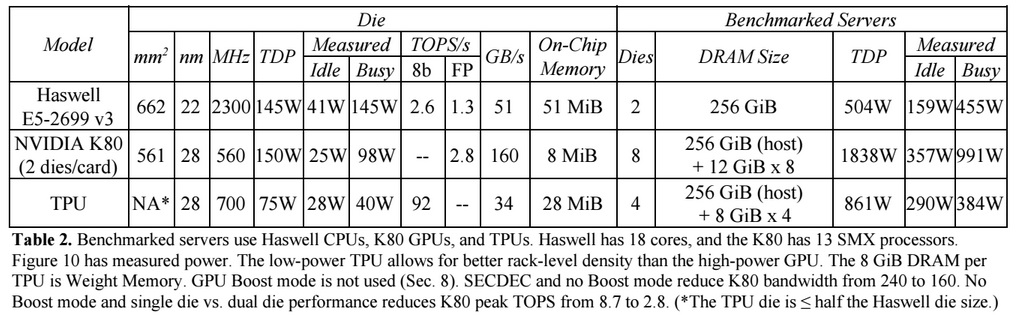
The Haswell E5 could do 2.6 tera operations per second (TOPS) using 8-bit integer operations running Google’s inferencing workload on its TensorFlow framework, while a single K80 die was capable of supporting 2.8 TOPS. The TPU did 92 TOPS on the inferencing work, blowing the CPU and GPU out of the water by a factor of 35.4X and 32.9X, respectively.
Benchmark tests are always welcomed, of course. And as Google knows full well, more data is always a wonderful thing. But the Keplers are two generations behind the current Pascals and this was not precisely a fair comparison to the GPUs, even if it does show the comparisons that Google must have been making when it decided to move ahead with the TPU project several years ago.
“We want to provide some perspective on Kepler,” Ian Buck, vice president of accelerated computing at Nvidia, tells The Next Platform. “Kepler was designed back in 2009 to solve traditional HPC problems, and was the architecture used in the “Titan” supercomputer at Oak Ridge National Laboratory. The K80 was one of many Kepler products that we built. The original research in deep learning on GPUs hadn’t even been attempted back when Kepler was designed. As soon as people started using GPUs for artificial intelligence, we started to optimize for both HPC and AI, and you can see that in the results we have had. For instance, the Tesla P40 using our Pascal GPU came out in 2016 just after the TPU was able to achieve 20X the AI deep learning performance than what we could do with K80. We think the TPU is a great validation for the need for these accelerators in the datacenter as Moore’s Law slows. Datacenters, whether running HPC or AI, need to look toward accelerated architectures to solve some of these problems.”
Nvidia has tweaked its high-end GPUs for compute a number of ways to support machine learning frameworks better, including variations aimed at both inferencing and machine learning. In November 2015, the only two Maxwell GPUs to make it into the Tesla accelerator family, the M4 and the M40, were announced. The M40 was specifically targeted at machine learning training, and had a single Maxwell GM200 accelerator with 3,072 cores running at 948 MHz that delivered 7 teraflops of single-precision floating point performance with a top thermal envelope of 250 watts. The much smaller Maxwell GM206 GPU, which has 1,024 CUDA cores running at 872 MHz, was used in the M4 accelerator aimed at machine learning inference workloads, and it delivered 2.2 teraflops single precision in a 75 watt peak power budget. The performance per watt of the M4 and M40 were essentially the same, but the M4 had only 4 GB of GDDR5 frame buffer memory for programs compared to 12 GB for the M40; it also had only 30 percent of the memory bandwidth of the M40 accelerator.
In June 2016, Nvidia put out the Pascal generation of accelerators aimed at machine learning, the P4 and P40, and in addition to half precision 16-bit floating point operations (FP16) and data sizes, the Pascal GPU used in these accelerators also supported the same 8-bit integer math operations (INT8) that Google uses in the TPU chip. (It is hard to believe that Google did not know that Nvidia planned to add 8-bit integer support to the Pascal chips, but by then, it had clearly made a decision to make its own TPUs for inference jobs). The P4 chip is based on the GP104 chip from Nvidia, and has 2,560 CUDA cores running at 810 MHz with 8 GB of GDDR5 memory, and with GPUBoost on running at 1.06 GHz and running in 8-bit integer mode, it has a peak theoretical performance of 21.8 TOPS running inference jobs – all in a peak thermal envelope of 75 watts. The fatter Tesla P40 accelerator is based on the GP102 Pascal GPU, with 3,840 CUDA cores running at a base 1.3 GHz with 24 GB of GDDR5 memory, and delivering a peak of 47 TOPS on inferencing workloads in a 250 watt thermal envelope.
In its paper, Google acknowledged that the P40 could deliver this 47 TOPS of inference performance, but had no idea what percentage of peak performance could be handled within the 10 millisecond response time for the 99th percentile of transactions that Google’s programmers wanted initially for its machine learning iron running inference jobs. The company did say that it could take a TPU implemented in 28 nanometer processes running at 700 GHz and operating within a 40 watt power envelope under load (75 watt thermal peak) and triple its performance by shifting from DDR main memory to the GDDR5 frame buffer memory used in various Tesla GPUs. All with only adding 10 watts more power to the card. (One wonders if there is not a follow-on TPU chip already doing this in Google’s infrastructure, then, seeing as though the TPU is obviously memory bandwidth constrained at only 34 GB/sec. Hmmmm. . . . )
Unhappy with the way that the TPU is stacking up against the GPUs that it sells, Nvidia ran some tests of its own using the open source GoogLeNet convolutional neural network application that is the best that Nvidia can do to approximate the inference workload that Google used in its tests. Here is how Nvidia ranks the K80 and the P40 against the Google TPU:
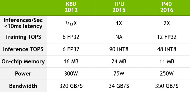
One weird thing in this chart that we can see right off the bat is that Nvidia is showing megabytes of on-chip memory instead of gigabytes of on-card accelerator memory. The P40 accelerator has 24 GB of GDDR5 memory for that GP102 chip to play with; each GK210B GPU on the K80 has 12 GB of GDDR5 memory hooked to it as well as 8 MB of on chip memory. The TPU has 28 MB of on chip memory as well as 32 GB of DDR3 memory wired onto the TPU card. This gigabytes of on-card memory is where the deep learning models are stored, so it is peculiar as to why the on-die memory is being highlighted here. Nvidia is also showing the peak performance of the TPU at 90 TOPS, when we know it is 92 TOPS from the Google paper, and the P40 accelerator at 48 TOPS in INT8 mode when we know it is 47 TOPS using Nvidia’s own specs. But set these aside for the moment.
What matters is that running the GoogLeNet inference workload with an average response time of under 10 milliseconds for the 99th percentile of transactions, the TPU could handle 280,000 inferences per second (IPS), as the paper pointed out, and the Pascal P40 could handle twice that number, or 560,000 IPS. (Why Nvidia did not print these numbers and used a multiplication factor is unclear.) A single GPU on the K80 card, as Google pointed out, was only able to process 36,465 IPS, or 1/13th that of the TPU, with that 10 millisecond cap for all but 1 percent of the transactions. We have no idea how to guess where the Tesla P4, which is in theory aimed more at inference workloads and which is in the same type of thermal envelope as the Google TPU stacks up. But let’s assume it can do the same ratio of GoogLeNet work as the P40 when reckoned against peak performance on INT8 jobs. That would put the Tesla P40 at 259,750 IPS, or essentially the same performance as the Google TPU for inferences with 10 millisecond or less response time for 99 percent of the transactions. If Google shifted to GDDR5 memory for its TPUs, it would add cost, but put it in the range of 840,000 IPS, and again, we suspect it might have already done this without telling anyone. (Shifting to DDR4 will not be enough of a bandwidth jump.)
The question one has to ask is what did Google pay to develop the TPU and then have it manufactured. Yes, the TPU allowed it to save massive amounts of money not doing inference on CPUs, which are clearly not as good at it as specialized processors are. But so what? If a P4 accelerator card costs $2,100 and if the P40 accelerator costs $4,700, which we think are the approximate street prices for these devices, then Google has to be able to make its own chip cost no more than this on a cost per watt per unit of performance basis for the TPU to make economic sense – and it has to cost less than this, presumably. If Nvidia can double the performance of machine learning inference with the future “Volta” GPUs that will presumably be announced at the GPU Technical Conference in May and possibly shipping later this year for selected HPC customers and maybe for AI customers, then Nvidia V4 and V40 accelerators will be in the same league as a TPU gussied up with GDDR5 memory and moved to a slightly more aggressive process shrink to 20 nanometers.
Google can afford to do anything, of course. But as it has pointed out in the past, the search engine giant only makes stuff when it can’t buy what it needs and total cost of ownership is the driving factor in its infrastructure decisions.
“The unit cost of a given amount of performance on GPU should be far less than a TPU,” says Buck, and as for beating them on the price of development and deployment, he defers any more questions to Google “For the rest of the market developing a custom ASIC for AI, it is an incredibly expensive and challenging task. We have been introducing new architectures to serve customers because the rate of innovation is fast. The culture here is to build and to execute quickly on something we want to accelerate and bring out as fast as possible. And we have been doing this at almost an annual rate. We are in the business to make accelerated computing easier to use and buy versus running all of this on commodity devices.”
The real question is how Google will be able to tweak its TensorFlow framework and its TPUs in lockstep to squeeze even more performance out of them. If it can’t do more than Moore’s Law, it might as well jump onto the GPU bandwagon or pick one of the interesting startups who are peddling all kinds of devices. And we will not be surprised if it does just that. We will also not be surprised if Google has some more TPU and TensorFlow tricks up its sleeves.