


There is nothing quite like great hardware to motivate people to create and tune software to take full advantage of it during a boom time. And as we have been saying since we first caught wind of the “Antares” Instinct MI300 family of GPUs, AMD is going to take Nvidia directly on in the generative AI market, and it is absolutely and unequivocally going to sell as many MI300A and MI300X GPU accelerators as it can make.
Nvidia should be thankful for the great fortune – and when we are talking about Big Green in the datacenter, we really do mean a great fortune – that demand for compute engines in the generative AI market is growing faster than the collective group of accelerators can supply. Because if this were not the case, and supplies of these complex and elegant devices were relatively unlimited and not being overpriced by voracious demand, then AMD would absolutely be stealing deals away from Nvidia with the GPUs and platforms it has put together based on the MI300 family.
As it turns out, such intense competition will be delayed as demand will probably exceed supply for AI training and heavy inference accelerators for the next one or two years. And the good news about that is that the supply shortages will allow all kinds of accelerator architectures to get some sort of footing – directly proportional to the large language models and tools supported and the number of accelerators that suppliers can get manufactured – that they might otherwise have not had. When supplies normalize and when all of the LLM and DLRM models have been tuned up by legions of software engineers for all kinds of devices, then there is going to be a shakeout and very likely a price war. In other words, the AI hardware market will return to something that resembles normal.
Until then, we all get to admire the hot rod iron that the accelerator chip makers are forging in their garages and setting loose for street racing at the hyperscalers, cloud builders, and HPC centers of the world, technology that eventually will trickle down to enterprises when it becomes more available and a hell of a lot cheaper per unit of work.
The Package Is More Important Than The Chip
What is fun for system architects and AI software developers right now, as the MI300s are being launched by AMD at its Advancing AI event in San Jose just down the road from Nvidia, Intel, and many AI accelerator makers, is that based on the raw feeds and speeds, the Demon MI300 systems built by Team Lisa Su can win by a nose and sometimes even more than that compared to the Hellcat H100 systems built by Team Jensen Huang.
Those Demon and Hellcat names refer to the top end Dodge Challenger muscle cars that The Next Platform is partial to – those are not AMD or Nvidia code names. (We know that Brad McCreadie, who used to run IBM’s Power processor development for many years and who moved to AMD five years ago to revamp its Instinct GPU designs and win exascale deals, loves Challengers and challenges.)
Depending on how you rank memory bandwidth alongside of raw compute, the Demon is the MI300X with 192 GB of HBM memory, 5.3 TB/sec of memory bandwidth, and 163.4 teraflops of FP64 matrix math in 750 watts, is the Demon. The new Nvidia H200, with 141 GB of HBM3e memory, 4.8 TB/sec of memory bandwidth, somewhere between 1.6X and 1.9X more effective FP64 matrix performance on real workloads than the H100, 66.9 teraflops of FP64 oomph in 700 watts, is the Hellcat. The AMD MI300A with 128 GB of HBM3 memory, 5.3 TB/sec of bandwidth, 122.6 teraflops of FP64 matrix math, in 760 watts would be the Challenger SRT, and the original Nvidia H100 with either 80 GB or 96 GB of HBM3, 3.35 GB/sec of memory bandwidth, 66.9 teraflops of FP64 matrix math in 700 watts would be the Challenger R/T Turbo in this extended analogy. We have little doubt that when Nvidia puts its “Blackwell” datacenter GPUs into the field next year, it will take the lead for a bit, but AMD is in the garage right now, too, forging the MI400.
Nvidia and AMD are going to push each other as much as customers are doing right now – and from here on out. And both are going to have market shares directly proportional to what they can ship out of the factories, and both are going to charge the same price per unit of work (more or less) for their GPUs depending on what metric above customers favor.
We are going to approach the MI300 announcement as we normally do, with a three pronged attack. First, in this article we will talk generally about the new AMD GPU accelerators and how they compare to prior generations of AMD devices. Then we will do a deep dive on the architecture of the MI300 devices, and then we will follow that up separately with a deeper competitive analysis between the AMD MI300A and the Nvidia GH200 Grace-Hopper hybrid and between the AMD MI300X and the Nvidia H100 and H200 accelerators. (It will take time to gather such information.)
As we already knew from the revelations that AMD made back in June, there are two versions of the MI300, with the MI300X being a GPU-only accelerator that is aimed at heavy AI training and inference for foundation models and the MI300A being a hybrid device mixing Epyc CPUs and Instinct GPUs on a single package and literally sharing the same HBM memory space, thus providing efficiencies for codes that still have some reliance on running serial code on the CPUs and flipping results over to the GPUs for more parallel processing.
Back then, we saw this note from the performance specs AMD was touting about the MI300 versus the MI250X, and as it turns out, this note sent us down a rathole that compelled us to overstate the performance of the MI300A as well as its power consumption. The note reads as follows:
“Measurements conducted by AMD Performance Labs as of Jun 7, 2022 on the current specification for the AMD Instinct™ MI300 APU (850W) accelerator designed with AMD CDNA™ 3 5nm FinFET process technology, projected to result in 2,507 TFLOPS estimated delivered FP8 with structured sparsity floating-point performance.”
That 850 watt statement made us think that AMD was overclocking the MI300A GPUs to get the same or slightly better performance on vector and matrix math than the MI300X, which presumably would run slower. This is not an unreasonable thing to think, given that the MI300A is going first into the “El Capitan” 2+ exaflops supercomputer at Lawrence Livermore National Laboratories and that this and other exascale “Shasta” Cray EX machines from Hewlett Packard Enterprise are water-cooled. As it turns out, the GPUs on the MI300A are not overclocked at all, and moreover, they don’t have slightly less memory bandwidth as their HBM capacity went down because there are not fewer memory stacks active (as happened with the first generation Hopper H100 GPUs) but rather shorter HBM memory stacks on the MI300A compared to the MI300X – eight chips per stack on the former, and twelve chips per stack on the latter, to be precise. So the MI300A turns out to be a lower than we had hoped on the compute performance and a little better on the memory bandwidth performance.
We would have still like to have seen El Capitan turbo charged with some overclocking. . . . Why not? This is the whole point of supercomputing, after all. That said, the effective performance of these chips on certain bandwidth bound workloads will be driven as much by memory as they are by raw compute.
Here is how the “Antares” MI300X and MI300A stack up against the prior AMD Instinct datacenter GPUs:
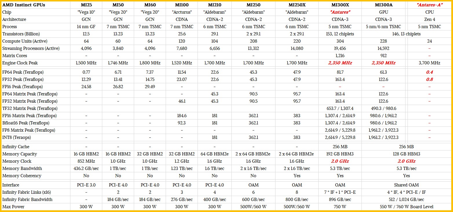
We are still waiting on the clock speed for the MI300X and MI300A GPU motors and their HBM3 memory, but we think these are in the right ballpark.
What is immediately obvious here is just how far AMD has come since the days of the MI25 and MI50, when Nvidia just completely and utterly controlled GPU compute in the datacenter. MI100 was a step in the right direction, MI200 was a tipping point, and MI300 is AMD coming into its own and bringing all kinds of technology to bear. What is not obvious from the table is how AMD’s chiplet approach and chiplet packaging comes to full fruition, using a mix of 2.5D chip interconnect with CoWoS interposers from Taiwan Semiconductor Manufacturing Co to interlink the MI300 compute complexes to HBM memory and 3D stacking of compute tiles – both CPU and GPU – atop Infinity Cache 3D vertical cache and I/O dies. This is 2.5D plus 3D packaging, what AMD calls 3.5D packaging.
We will get into the packaging details in our forthcoming architectural deep dive. For now, let’s just go through the feeds and speeds for compute, memory, and I/O on these two AMD compute engines and talk a bit about how they compare to the prior generation specifically. We will begin with the compute on the full-on MI300X discrete accelerator:
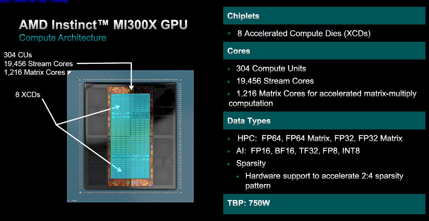
The MI300X has eight Accelerated Compute Dies, or XCDs in the AMD lingo. Each XCD has 40 compute units, but only 36 of them are exposed to the outside world at the time to increase the effective yield on the 5 nanometer chiplets. There is another 10 percent of performance latent in the design, and we would not be surprised to see full yield versions productized at some point.
Add it all up, there are 304 compute units across the MI300X, with 19,456 stream cores doing vector math and 1,216 matrix cores doing matrix math. The matrix cores – what most people call tensor cores – support 2:4 sparsity to boil down sparse matrices to dense ones do effectively double their throughput. The vector engines do not have sparsity support. As you can see from the chart above, all of the necessary data formats are supported on the MI300X, and the same formats are supported by the MI300A.
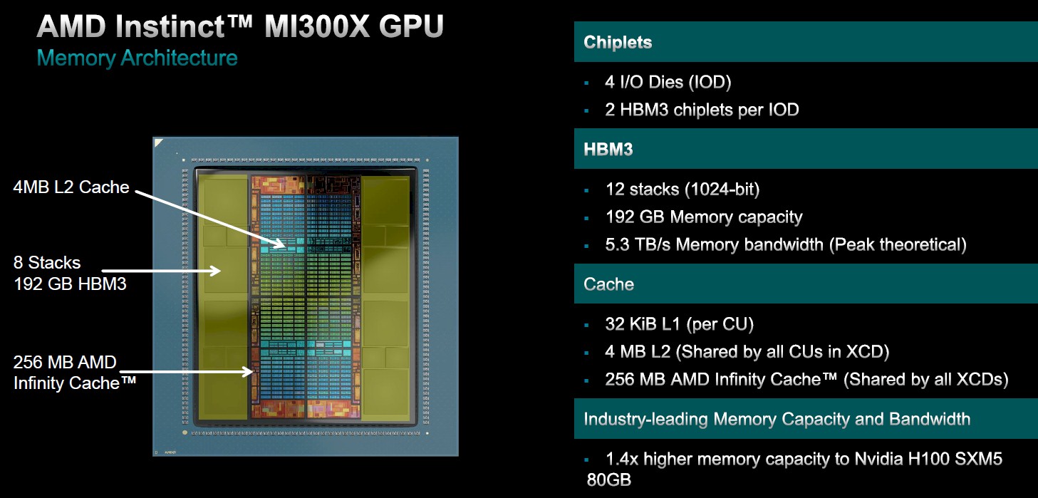
For memory, each MI300X compute unit has 32 KB of L1 cache, and there is a 4 MB L2 cache shared by all of the compute units in each XCD and a further 256 MB Infinity Cache shared by all of the XCDs in the MI300X complex. There are eight stacks of HBM3 memory attached to the I/O dies – two controllers for each of the four I/O dies – and the little squares between each pair of HBM3 banks are just spacers to aid in the manufacturing of the MI300X complex. The HBM3 stacks are twelve chips high at 2 GB per chip, which gives 192 GB of total memory and the 5.6 TB/sec of bandwidth.
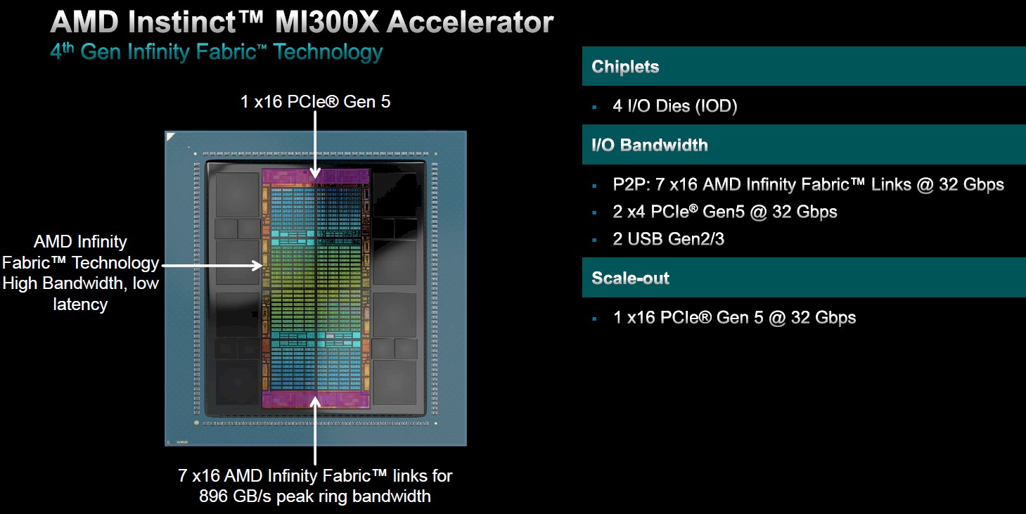
The four underlying I/O dies, or IODs in the AMD lingo, have seven Infinity Fabric links with a combined peak ring bandwidth of 896 GB/sec of bandwidth to glue eight MI300Xs into a single, shared memory, virtual GPU. There is one PCI-Express 5.0 x16 port coming off the complex to link to external networks and systems. All told, there is 1 TB/sec of aggregate I/O bandwidth in the MI300X complex.
Here is how the MI300X compares to the prior MI250X
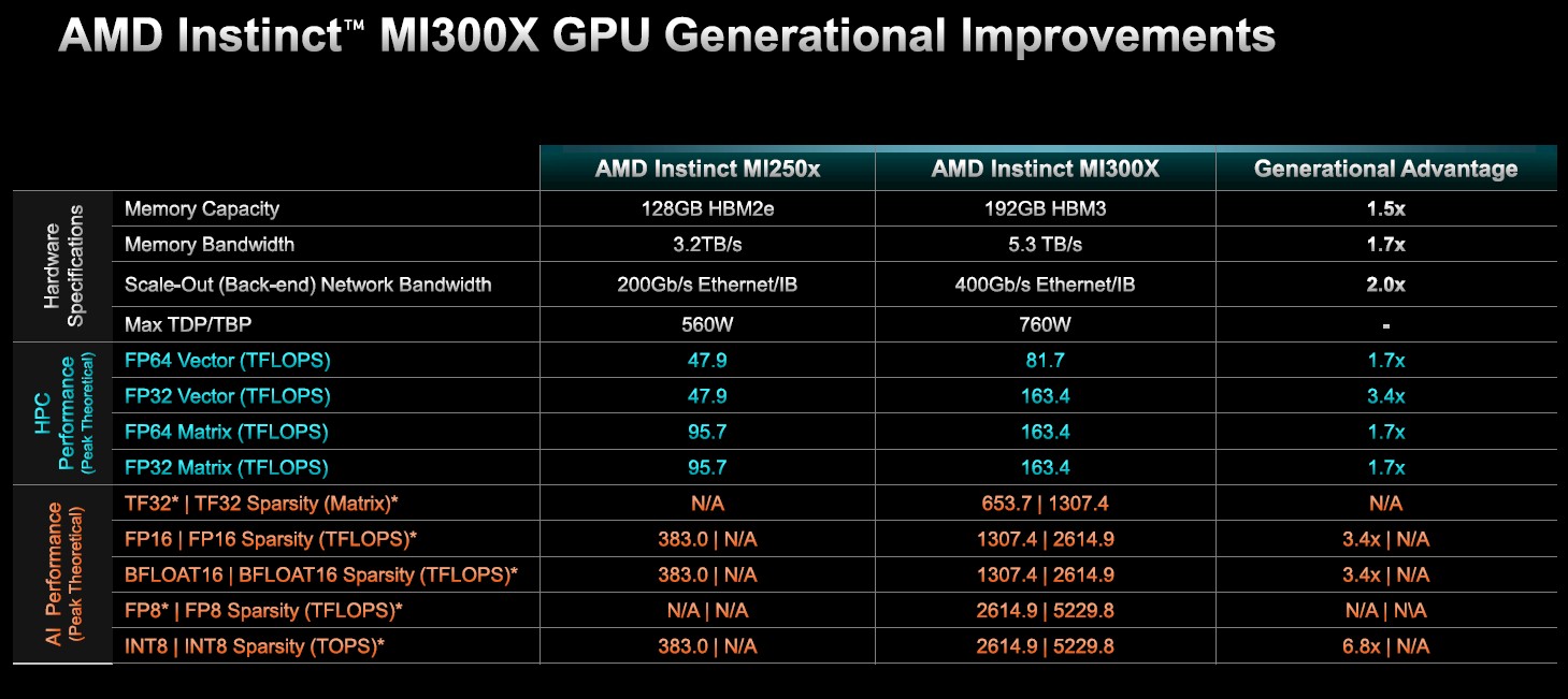
You get 1.7X or 3.4X more performance (the FP32 has tweaks to double its performance, and there is sparsity support on the matrix engines, which is why it is 3.4X there) against 1.5X more main memory, 1.7X more bandwidth, with 2X the external network bandwidth, against a 35.6 percent increase in heat.
That is called engineering. Industry luminaries say that packaging is the next lever in the evolution of compute, and nothing demonstrates this so well as the MI300X and its sibling MI300A.
With the MI300A, you pry off two GPU chiplets and lay down three eight-core “Genoa” Epyc 9004 chiplets and create a shared compute complex where both GPU and CPU can address the same memory and not have to pass data back and forth over some kind of bus or interconnect.
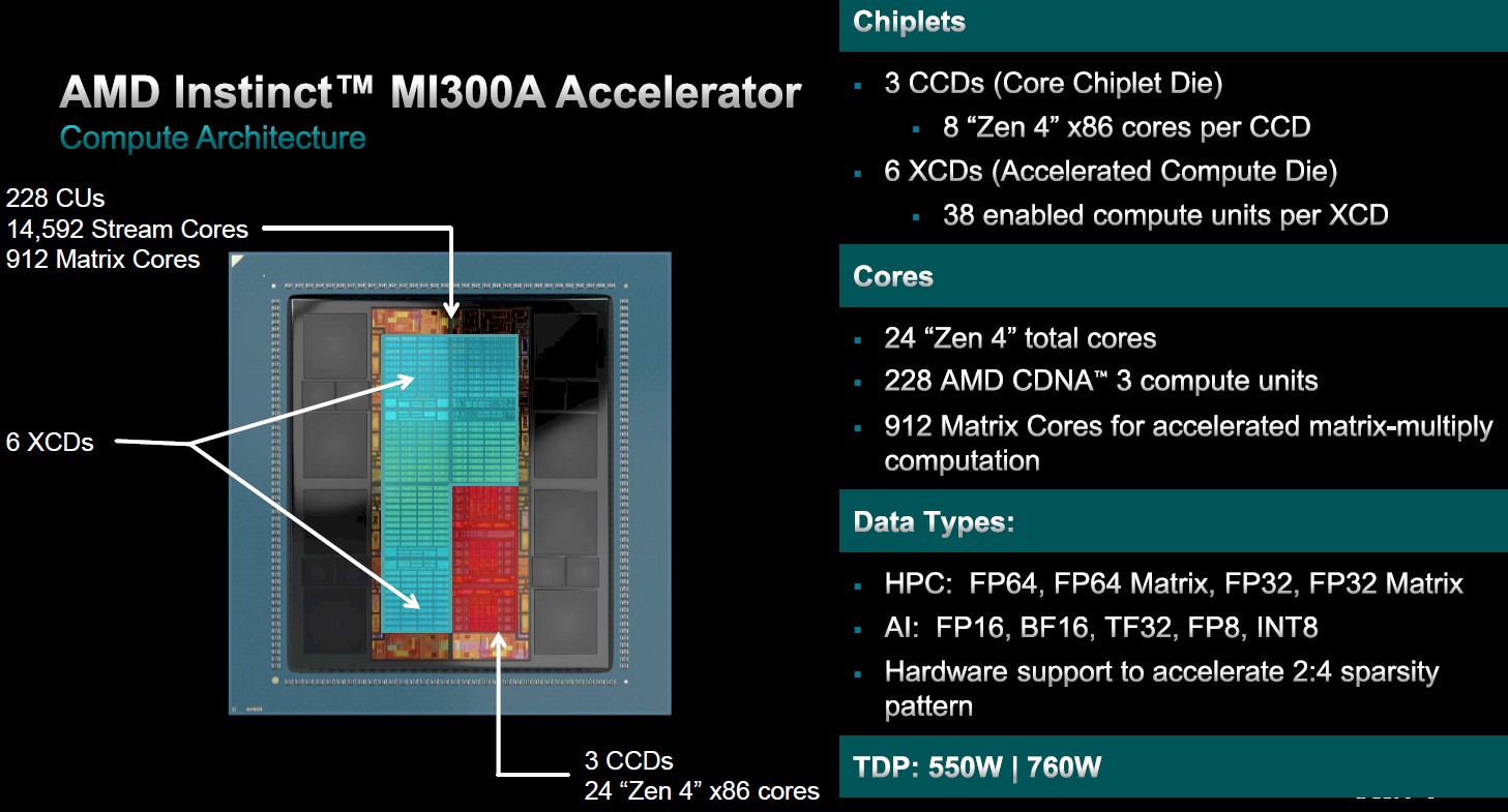
The MI300X has 228 compute units, with a total of 14,592 stream cores and 912 matrix cores across six XCDs. The chip complex is rated at 550 watts and the board package using the MI300A weighs in at 760 watts.
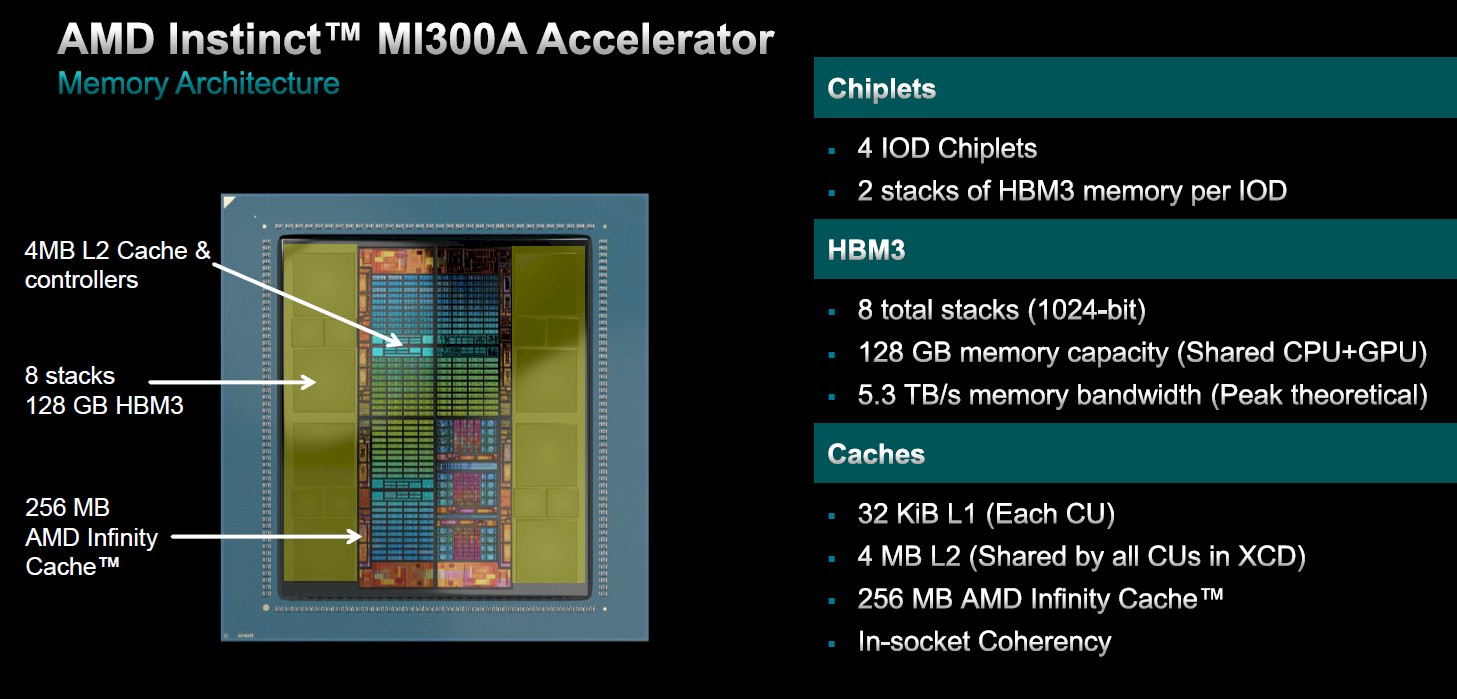
The cache memory om the MI300A complex is the same as on the MI300X, but the HBM3 memory stacks are only eight chips high compared to the twelve on the MI300X, which is why the memory comes in at only 128 GB. The trimming of the memory was done to curb power draw, heat, and cost – all of which the traditional HPC market is sensitive to.
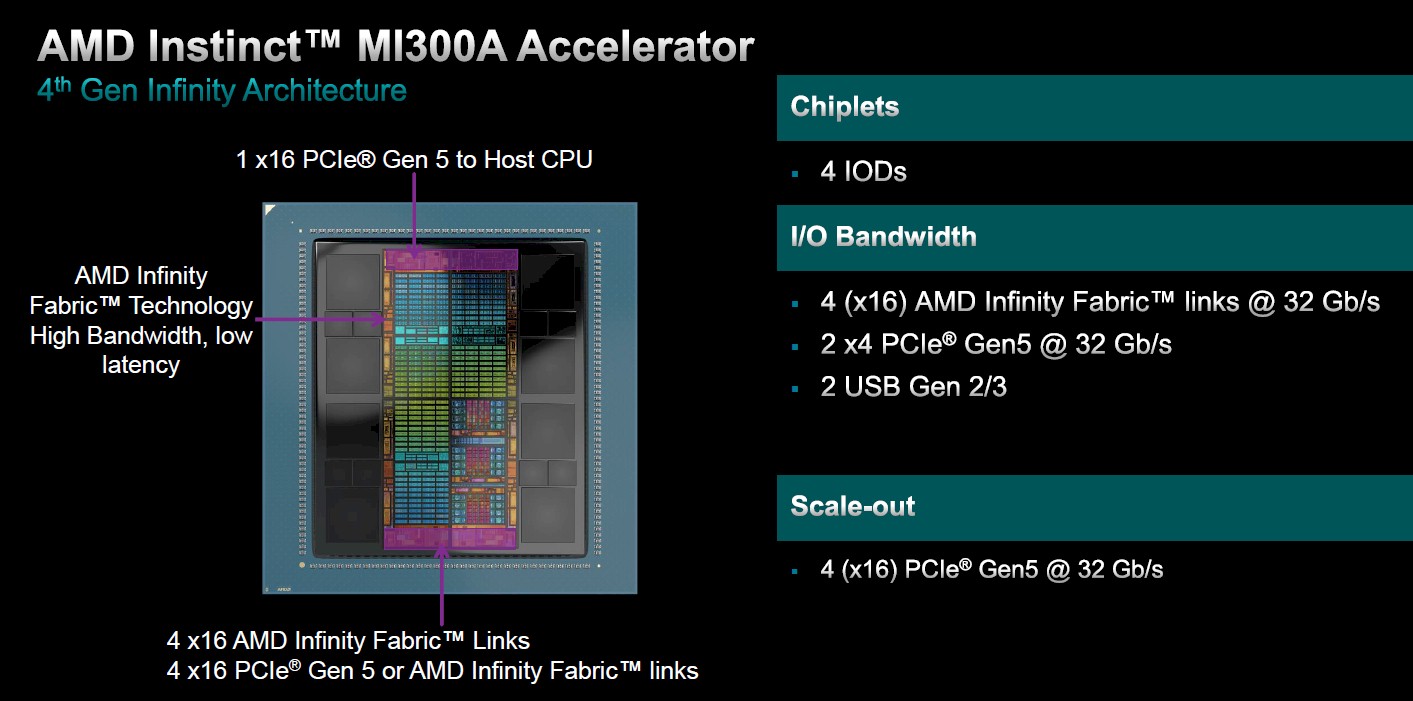
The I/O on the MI300A is a little different from the MI300X as well. There are four Infinity Fabric links with 512 GB/sec of bandwidth and another four links with 512 GB/sec of bandwidth that can be used as either four PCI-Express 5.0 x16 links or as four additional Infinity Fabric links. This configurability allows for a setup with four tightly coupled MI300A CPU-GPU complexes with four fat pipes for additional I/O or a higher number of GPUs with less I/O.
Stack it all up, and here is how the MI300A compares to the MI250X:
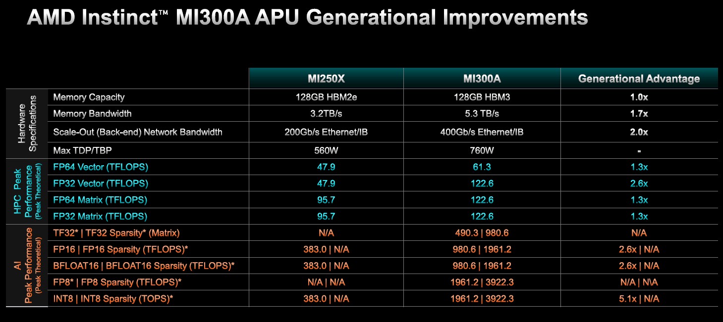
The HBM memory capacity is the same between these two devices, but the HBM memory bandwidth is 1.7X higher and is literally shared by the GPU and CPU chiplets. The external interconnect speed is doubled against a 1.3X to 2.6X increase in peak theoretical performance for the same 35.6 percent increase in power.
We look forward to seeing how this shared memory affects real-world application performance for both HPC and AI workloads.
The Platform Is More Important Than The Package
Ultimately, what customers buy are platforms, not chips or sockets, and AMD says that the MI300X GPUs plus into the same Open Compute Universal Baseboard (UBB) system boards that were created for the same MI200 series.
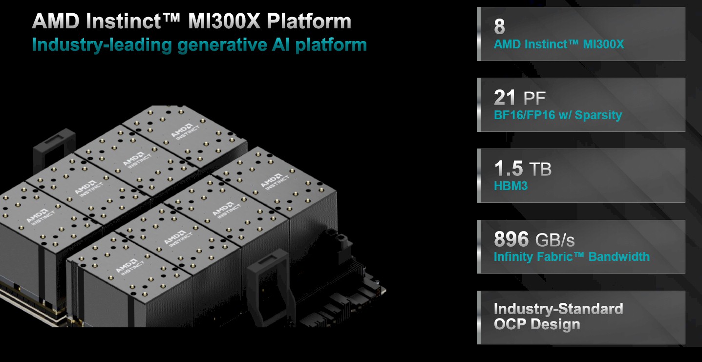
With eight MI300X devices lashed together, a single UBB complex can deliver 21 petaflops at BF16/FP16 precision with sparsity on (obviously 10.5 petaflops for dense data), with a combined 1.5 TB of HBM3 memory and 896 GB/sec of Infinity Fabric bandwidth between the GPUs and one fat PCI-Express 5.0 x16 pipe to the outside world. Meaning, a CPU, that in turn has access to the network fabric linking multiple nodes together in a cluster.