
Rambus recently announced the availability of its new High Bandwidth Memory (HBM) Gen2 PHY. Designed for systems that require low latency and high bandwidth memory, the Rambus HBM PHY, built on the GLOBALFOUNDRIES advanced 14nm Power Plus (LPP) process technology, is targeted at networking and data center applications.
According to Frank Ferro, a senior director of product management at Rambus, HBM is a high-performance memory that features reduced power consumption and a small form factor. More specifically, it combines 2.5D packaging with a wider interface at a lower clock speed (as compared to DDR4) to deliver higher overall throughput at a higher bandwidth-per-watt efficiency for high-performance computing applications.
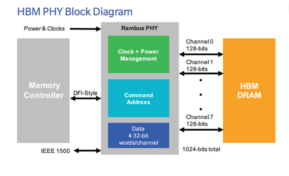
“The Rambus HBM Gen2 PHY, which is fully compliant with the JEDEC HBM2 standard, supports data rates up to 2000 Mbps per data pin, resulting in a total bandwidth of 256 GB/s,” he explained. “The interface features 8 independent channels, each containing 128 bits for a total data width of 1024 bits, as well as support for a stack height of 2, 4 or 8 DRAMs. The PHY is also designed for a 2.5D system with an interposer for routing signals between the DRAM and PHY.”
This combination of signal density and stacked form factor, says Ferro, requires special design consideration.
“To enable easy implementation and improved flexibility of design, Rambus performs complete signal and power integrity analysis on the entire 2.5D system to ensure that all signal, power and thermal requirements are met,” he concluded.
The HBM Gen2 PHY – delivered as a fully characterized hard macro – includes all necessary components for robust operation, such as IO pads, PLL, clock distribution, transmit and receive paths, control logic, power distribution and electrostatic discharge (ESD) protection circuitry.
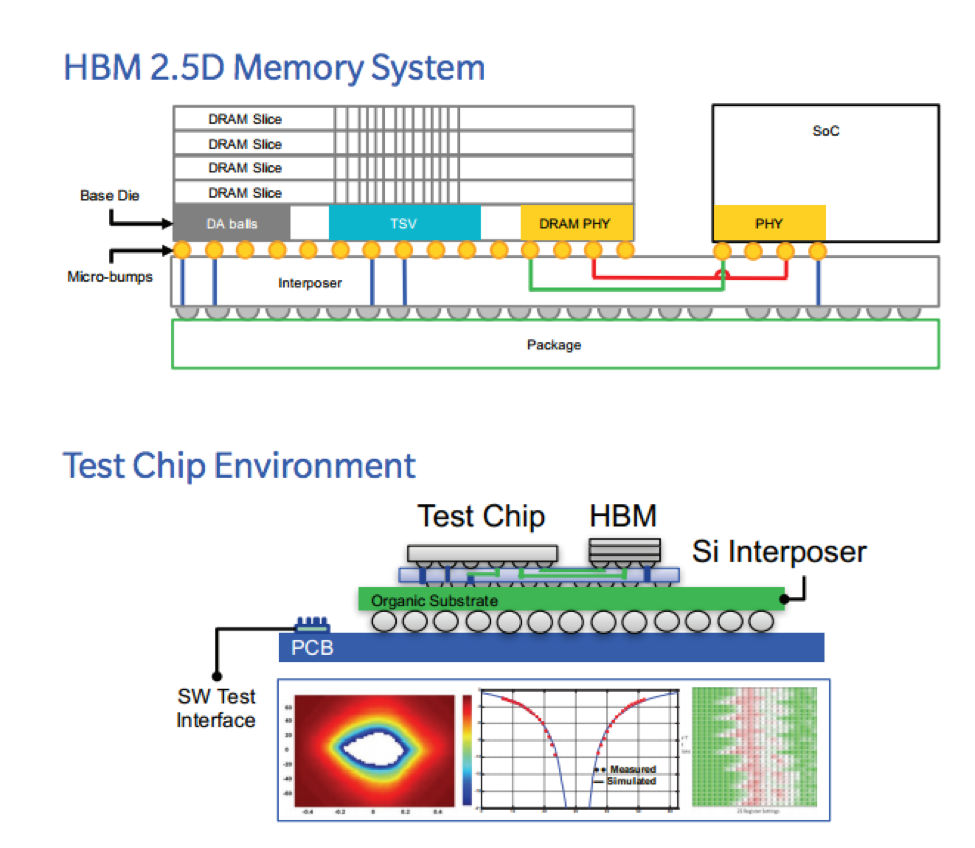
Key HBM Gen2 PHY product highlights include support for DRAM 2, 4 and 8 stack height, a DFI-style interface to the memory controller, 2.5D interposer connections between the PHY and DRAM, a validated memory controller interface, support for wafer-level and interposer testing, as well as availability with LabStation™ Validation Platform for enhanced bring-up and validation.
Additional features include a flexible delivery of the IP core (works with ASIC/ SoC layout requirements), 8 channels and 16 pseudo-channels, selectable low-power operating states, programmable output impedance, pin programmable support for lane repair, ZQ calibration of output impedance, IEEE 1500 test support, SSO noise reduction, micro-bump pitch matched to the DRAM pitch, east-west orientation (PHY can be placed in corner of die) and a register interface for state observation.
Interested in learning more about Rambus’ HBM Gen2 PHY? You can check out our product page here and download our product brief here.