


Here at The Next Platform, the quarterly earnings season starts with Taiwan Semiconductor Manufacturing Co. And that is fitting given the utter dependence that the world has on the chip manufacturing and packaging processes that this company sells at a profitability that not only allows it to invest prodigiously in the future technologies, but to pay handsome returns in share price rises and dividends.
It is hard to figure how Intel Foundry in the United States or Semiconductor Manufacturing International Corp in China will ever catch up, and it may even be likely that TSMC’s operations in the United States will come to dominate the upper echelon in chip making in the US over the next few years – much to the chagrin of Intel and its new chief executive officer Lip-Bu Tan.
That said, Taiwan will still have the dominant slice of TSMC’s fab capacity, although chip designers in the United States and Europe will no doubt be comforted that should anything disrupt operations in Hsinchu and Kaohsiung Science Parks on the island nation, there will be capacity available.
CC Wei, TSMC’s chief executive officer, reminded Wall Street analysts of the scope of the buildout in the United States and Taiwan over the coming years, plus two specialty fabs in Japan and one in Germany, on a call going over the financial results for the second quarter of 2025.
In the United States, TSMC has committed to spending $165 billion for six chip fabs, two advanced packaging fabs, and a research and design center to support customers in North America, all in the Phoenix suburbs of Arizona. Two of these fabs are going to be coming online early “by several quarters,” according to Wei.
The first TSMC fab in Arizona started full production in the fourth quarter of last year, and is etching chips with 4 nanometer N4 processes. The second fab is focused on N3 processes, which etch at 3 nanometers, and it is completed and this is the one that customers want TSMC to ramp up early. The third Arizona fab will use N2 and kicker A16 processes, which as the names suggest support 2 nanometer and 16 angstrom (1.6 nanometer) processes, is already under construction, and TSMC is looking to speed up its production schedule given demand for advanced processes for AI compute engines for both training and inference. The fourth fab for TSMC in Arizona will use equipment that etches with using the N2 and kicker A16 processes. The fifth and sixth fabs will use smaller transistor geometries, presumably the A14 processes and then downwards from there.
When all is said and done, about 30 percent of the chip making capacity at 2 nanometers and smaller geometries will be located in Arizona. TSMC operates nine chip factories today in Taiwan. The Fab12 in Hsinchu, Fab 14 and Fab 18 in Tainan, and Fab 15 in Taichung do twelve-inch (300 mm) wafers and can etch anywhere from 130 nanometers down to 3 nanometers, depending on the machinery installed in each facility. These are known collectively as the “gigafactory,” and they are designed to be able to dial up and down N7, N5, and N3 node capacity and will be able to handle N2 node output as well without having to massively reconfigure the machinery. Fab 20 in Hsinchu and Fab 22 in Kaohsiung are bringing up 2 nanometer processes right now.
Wei said that with the support of the Taiwanese government, TSMC will build eleven fabs and four packaging facilities over the next several years, which presumably will require an even larger investment than the $165 billion being spent in the US to build out fab capacity. No number has been given for this fab expansion in Taiwan.
“We expect the number of new tapeouts for 2 nanometer technology in the first two years to be higher than both 3 nanometers and 5 nanometers in the first two years, fueled by both smartphone and HPC applications,” Wei explained on the call. The base N2 process will, he added, deliver 15 percent higher transistor density of the enhanced N3E process that is currently shipping for high-end devices, and 10 percent to 15 percent higher transistor switching speeds at the same power, or 20 percent to 30 percent lower power at the same performance. A16, which is akin to the jump from N4 to N4, will provide 7 percent to 10 percent transistor density improvements and either an 8 percent to 10 percent speed bump or a 15 percent to 20 percent energy efficiency improvement at the same performance. A16 enters volume production in the second half of 2026, and Wei said that it is best for “specific HPC products with complex signal routes and a dense power delivery network.”
It will be interesting to see which chips wait for A16 and which ones can’t wait and end up on N2. The A14 process will push the transistor envelope a little further, with providing the same performance and thermal bump that N2 did compared to N3, with a slightly higher transistor density delta (20 percent instead of 15 percent) when it starts ramping in 2028.
Wei said that capacity for both the N5 and the N3 nodes was “very tight” in the second quarter of this year. High demand drives up the revenues and, presumably, unit prices. Or it at least is supposed to according to idealized economic theory that often doesn’t pan out in a real world where people get miffed if you gouge opportunistically on prices.
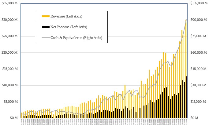
In the second quarter, TSMC set revenue and income records, and there is no reason to believe that it will not keep doing this in the years ahead as demand for PCs and generic servers and smartphones is more or less stable and demand for AI compute engines is skyrocketing.
In the quarter ended in June, TSMC booked $30.07 billion in sales, up 44.4 percent year on year and up 17.8 percent sequentially. Net income came in at $12.8 billion, which represented a whopping 42.6 percent of revenues and which increased 67.2 percent from Q2 2024.
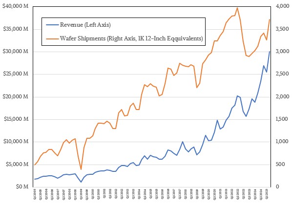
Wafer shipments, as measured in 12-inch silicon wafer equivalents (some production on older processes is still done on 8-inch wafers), rose by 19 percent to 3.72 million in the quarter. Revenue per wafer, which is driven by the complexity of the chips and the packages that TSMC makes on behalf of its customers, keeps on rising, and was up 21.4 percent in Q2 to $8,088 per 12-inch equivalent wafer. That is double the revenue from a wafer in Q2 2019
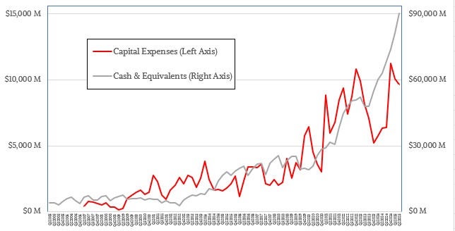
TSMC ended the quarter with $90.36 billion in cash and investments, which is a pretty hefty down payment on its ambitious capital expense plans in the US and Taiwan. (The foundries in Germany and Japan are fairly modest.)
The N3 ramp is well under way, as you can see in the chart below:
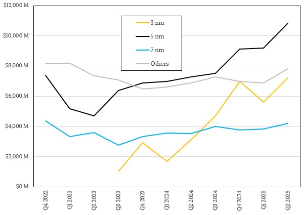
In the quarter, sales of devices etched with 3 nanometer processes accounted for $7.22 billion, up 2.31X from the year ago period. Revenues from 5 nanometer chips (which include 5N and 4N process variants) hit $10.83 billion, up 48.5 percent. And 7 nanometer chips were humming along with $4.21 billion in sales up 18.9 percent. All other etching on larger transistor densities combined contributed 26 percent of revenues, which is $7.82 billion and which was up 13.8 percent year on year. Some very old processes persist because they are cheap and many kinds of chips don’t benefit enough from being shrank to justify the much higher cost of design and production.
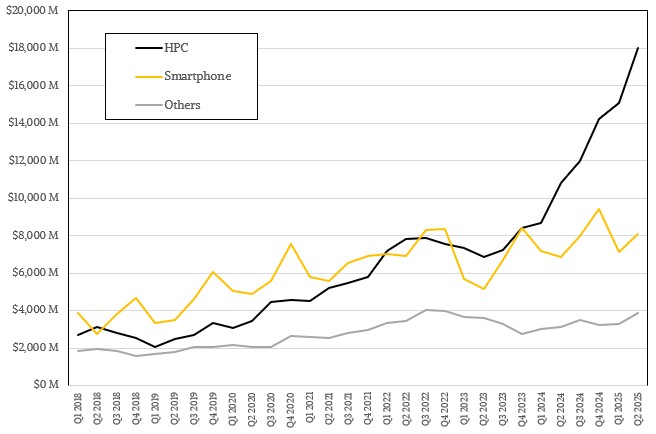
The so-called “HPC” devices that TSMC makes, which includes any high performance CPU, GPU, network, or storage ASIC, drove a little more than $18 billion in sales, up 66.6 percent year on year and up 19.8 percent sequentially from Q1 2025. Smartphones, which for the longest time were the big drives of process and revenues at TSMC, stopped being the big driver a year and a half ago. In the current quarter, the making of smartphone chips brought in $8.12 billion in sales, up 18.2 percent. Other kinds of chips accounted for $3.91 billion in sales, up 25.2 percent.
For a while there, TSMC was giving out hints about how much of its revenues were being driven by AI inference and training chips, and we built a model about this. The company has not said much in this regard for a few quarters – perhaps it is letting on too much about the high margins that some chip makers are commanding for their chippery – but we continue to make our estimates, as you can see below:

Our best guess is that AI chip manufacturing and packaging drove $8.78 billion in revenues for TSMC in the second quarter, up by a factor of 3.67X year on year. Other HPC chips drove $9.26 billion in sales, up a mere 9.8 percent. And we think some of this was for AI switch and network interface ASICs, which presumably were not on the AI training and inference chip numbers that TSMC had been talking about vaguely in the past.
The upshot is that AI is driving about a third of TSMC’s revenues, more or less. And it will not be long before it is driving half. And no, we are not counting AI CPUs for PCs and smartphones as being driven by AI – that is a given, not a driven. Very few people would pay for these extra functions, but they will take them for free.