

After nearly six decades of getting smaller, faster, cooler, and cheaper, transistors are getting more and more expensive with each generation, and one could argue that this, more than any other factor, is going to drive system architecture choices for the foreseeable future.
Either the reticle size of fab equipment is going to limit us, or the internetworking between components, whether they are on a single socket in 2D, 2.5D, or 3D configurations, is going to limit us. We find chiplet architectures perhaps unavoidable as well as interesting, and we admit that chiplet approaches have the potential to increase individual component yields and therefore reduce semiconductor costs, but the use of chiplets also increases package manufacturing costs and there is a price – and potentially a very large price in computational efficiency and thermals – of not having monolithic compute elements very close to their cache and main memories.
Perhaps we should have invested a little bit more in 450 millimeter wafer technology? Maybe not. The silicon ingots that wafers are sliced from are 3X heavier and take 2X to 4X the time to cool, and all of the machinery in a modern fab that automatically handles the wafers during the manufacturing process would have to be changed along with the etching equipment.
Some days, it seems that 3D stacking of compute and memory is the only way out of this conundrum, and even that has huge engineering and economic challenges.
It is with this in mind that we read a new paper published in the online journal for the Society for Industrial and Applied Mathematics written by Satoshi Matsuoka, director of the RIKEN supercomputing lab in Japan and a longtime professor at the Tokyo Institute of Technology, and Jens Domke, the leader of the supercomputing performance research team at RIKEN, that talked theoretically about supercomputing design in the wake of the “Fugaku” system delivered last year and as the end of Moore’s Law approaches.
We think Matsuoka and Domke are being generous in that it sure looks like Moore’s Law is kaput. Finito. No mas. Fini. Joined the choir eternal. Gone the way of all flesh. Yes, transistor density is still increasing and will continue to increase, but that was never the point that Intel co-founder Moore was making in his seminal papers in 1965 and 1975. The point was that ever-cheapening transistors would drive the computing industry forward, at an exponential rate, which certainly happened.
Until now. Now, everything is harder. And hotter. And more expensive. And until we can reach down into the microcode of the BIOS of the physical Universe and change some fundamental laws, that si just the way it is with CMOS semiconductor technology etched on silicon wafers.
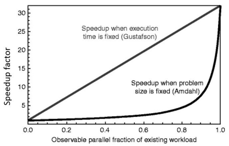
To recap: Amdahl’s Law has many phrasings and was coined by Gene Amdahl, the legendary architect of the System/360 mainframe at IBM. The one we were taught was that a system is only as fast as its slowest component. The idea was presented by Amdahl at the 1967 spring conference of the American Federation of Information Processing Societies as such: “The overall performance improvement gained by optimizing a single part of a system is limited by the fraction of time that the improved part is actually used.” The more parallel the application, the greater the speedup, which is what is commonly called strong scaling in the HPC arena.
Like many great ideas, it seems obvious once stated, but Amdahl’s Law has huge implications for high performance computing of all kinds, not just simulation and modeling.
So does Gustafson’s Law, which was presented in a 1988 article at the Association of Computing Machinery called Reevaluating Amdahl’s Law, by HPC legend and applied mathematician John Gustafson and Edwin Barsis, who was the director of computer sciences and mathematics at Sandia National Laboratories when this paper came out and Gustafson was working at Sandia.
Gustafson’s Law is akin to Special Relativity, where Amdahl’s Law is more like General Relativity, if a metaphor is required. Amdahl’s Law was about how a fixed problem scales on changing hardware, but the Sandia team focused on how a changing problem scaled on changing hardware and could provide greater resolution of simulation over time – and tried to formulate a way to gauge the efficiency of all of that. One of its assumptions is that the serial portion of workloads does not grow even as the parallel portions do.
There is a fascinating writeup in the New York Times about the parallel computing algorithm breakthrough at Sandia, which is one of the few references to Barsis on the Internet. And, quoting Barsis, it gives a very nice description of the weak scaling principle of Gustafson’s Law: “We don’t keep breaking up the parallel part smaller and smaller and smaller. We keep making the total problem bigger and bigger and bigger.”
What a poetic way to describe the past three and a half decades of HPC and to capture the spirit of Gustafson’s Law. Which is all about cheating Amdahl’s Law as much as possible through clever hardware and software engineering.
Which brings us all the way back to RIKEN Lab and the post-Fugaku world, the paper at SIAM, and a presentation by Matsuoka at the recent Modsim Workshop hosted by Brookhaven National Laboratory.
Here is a chart Matsuoka pulled from a lecture series by Peter Bermel at Purdue University that shows the interplay of these two laws in 2D:
And here is a beautiful 3D chart put together by Matsuoka and Domke for the SIAM article:
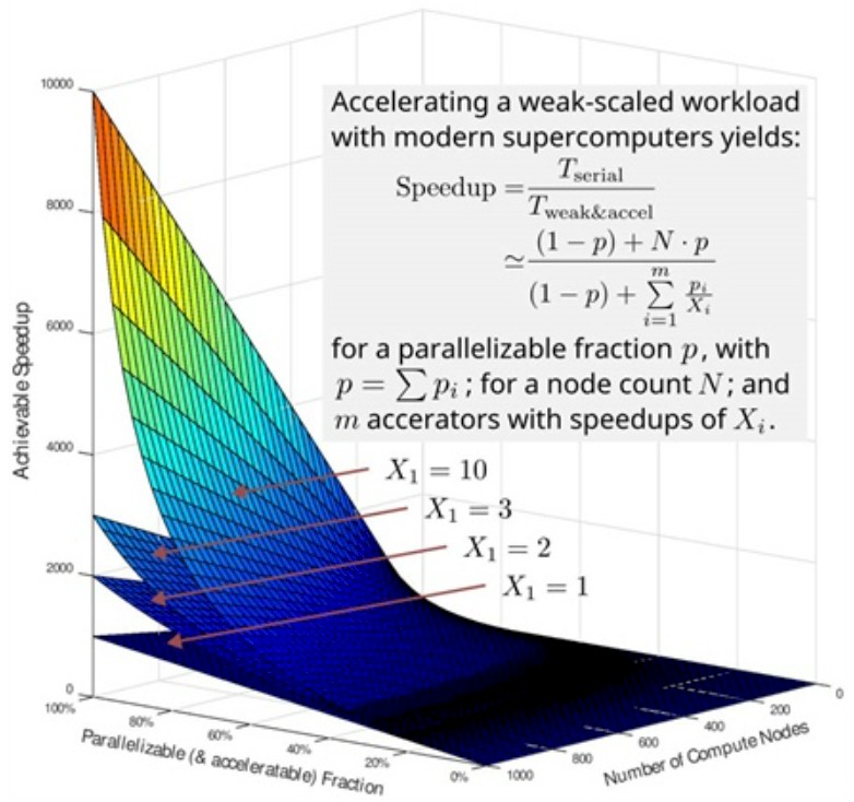
“The supercomputing community typically regards Amdahl’s Law as the strong-scaling law under which the use of more compute nodes accelerates a given parallelizable fraction of the workload and reduces the time to solution,” Matsuoka and Domke write in the SIAM paper. “But this law also applies to accelerators, and the potential speedup is bound by the ratio of accelerated and non-accelerable fractions of the algorithm. Furthermore, a second fundamental observation called Gustafson’s Law also governs modern HPC by limiting the achievable speedup for a problem based on how well the parallelizable or accelerable fraction can be weak scaled onto many nodes; one accomplishes this by increasing the overall workload and maintaining a constant amount of work per node. Weak scaling overcomes a problem’s bottlenecks – slowdowns due to communication issues with the interconnection network or inherent imbalances in the workload distribution – that become evident when one strong-scales to the same number of compute nodes.”
The gist of that second chart above, say the authors, is that a perfect accelerator can yield “a significant speedup,” which is on the order of 10,000X on the chart above, but that any Amdahl’s Law inefficiencies within the accelerator and any Gustafson’s Law inefficiencies across distributed collections of accelerators and data transfers between compute nodes all hold back scalability. And you can quantify this before you design a next-generation supercomputer. Which is what Matsuoka’s lengthy and detailed presentation at Modsim 2022 was all about. (We have not been able to secure a recording of the session, just the presentation, which is a fascinating read in itself.)
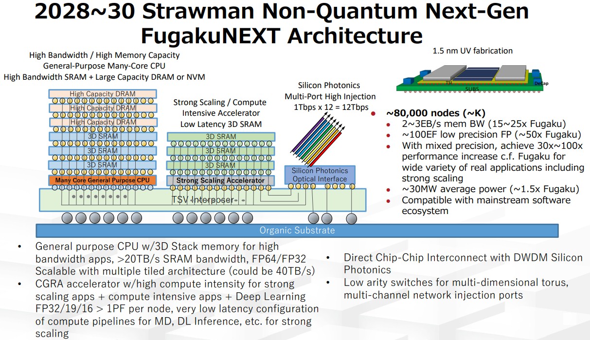
And this brings us all the way back to the FugakuNext strawman hypothetical proposal for a next-generation supercomputer for RIKEN expected between 2028 and 2030, which we covered a bit back in April when a paper from RIKEN and a bunch of other university researchers around the globe, worked together to benchmarks HPC performance on the AMD Milan-X Epyc 7773X large cache processors. As it turns out, there are now two FukaguNext strawmen in the field, one that is an accelerated CPU (like A64FX) with lots of stacked L2 cache and another, which Matsuoka showed in his Modsim 2022 presentation, that is a hybrid CPU/accelerator device that has tons of 3D stacked memory and cache on the devices to provide strong scaling.
Those initial AMD Milan-X tests, using the MiniFE finite element analysis application, proved that with a dataset that fit inside the L3 cache, MiniFE routines ran 3X faster. The large cache reduces a big Amdahl’s Law bottleneck – main memory. In other words, last level cache – either L2 cache or L3 cache, depending on the architecture – is the new main memory. Suddenly, we are having flashbacks to the servers of the late 1990s. . . .
Anyway, RIKEN then extrapolated what a future A64FX processor with a ton of stacked L2 cache might look like and how it might perform. This A64FX large cache (LARC) processor was simulated with eight L2 caches stacked up atop the A64FXNext processor with 384 MB of L2 cache at 1.5 GB/sec of bandwidth, and was modeled to yield an average of 10X improvement in the performance of a FugakuNext socket over a current Fugaku socket.
Pretty, isn’t it? And it is not a CPU with beefy vector engines like the A64FX. Not that RIKEN has made a decision one way or the other on that as yet. These two strawmen systems are just thought experiments for now. But they will inform proposals and design decisions, for sure.
This prospective hybrid FugakuNext compute engine has a general purpose CPU – no doubt based on the Arm architecture – and has a coarse-grained reconfigurable array (CGRA) accelerator. These could be, according to Matsuoka, a GPU with clock-level synchronization, an FPGA fabric like those from Xilinx or Intel, or the Intel dataflow engine called the Configurable Spatial Architecture, or CSA, that we caught wind of in patent filings way back in 2018.
You will also note that there are 2D SRAM caches stacked on top of both the CPU and the accelerator, and that the CPU has DRAM stacked on top of the SRAM. The interposer also has twelve ports of 1 Tb/sec silicon photonics networking coming right off the package. RIKEN reckons that this chippery will be etched in 1.5 nanometer processes.
This potential FugakuNext socket would have more than 1 petaflops of performance per node at FP16 precision, which probably means more than 500 teraflops at FP32 single precision and 250 teraflops at FP64 double precision, and greater than 20 TB/sec of memory bandwidth of SRAM bandwidth. This potential FugakuNext system would have around 80,000 nodes with somewhere between 2 EB/sec and 3 EB/sec of aggregate memory bandwidth, around 100 exaflops of mixed precision performance, and burn around 30 megawatts of juice.
This sounds pretty reasonable as a wish. Question is: Can it be made, and can anyone afford to make it?

Thanks for this detailed update on A64FX developments! Vertical cache sounds great for HPC and the CGRA could benefit that as well as datacenters and clouds. These coarsely reconfigurable accelerators are probably better suited to pairing with CPUs in these systems (Cortex-X? Xeon-W?) than FPGAS whose use demands time-consuming HDL coding, place-and-route, timing analysis, and bitstream uploads. I think that those coarse-grained units are meant to allow quick reconfigurations particularily for common foundation models of ML/AI, providing the desired application-specific acceleration (language, vision, cognition, …), beyond what a “general-purpose” GPU may do, and more readily than with FPGAs. Great writeup!
https://www.bnl.gov/modsim2022/files/talks/satoshi-matsuoka.pdf super interesting – begs the inevitable question though – does it run Crysis?