

The 3D stacking of chips has been the subject of much speculation and innovation in the past decade, and we will be the first to admit that we have been mostly thinking about this as a way to cram more capacity into a given compute engine while at the same time getting components closer together along the Z axis and not just working in 2D anymore down on the X and Y axes.
It was extremely interesting to see, then, the 3D wafer-on-wafer stacking that AI chip and system upstart Graphcore has been working on with Taiwan Semiconductor Manufacturing Co had nothing to do making logic circuits more dense within a socket. This will happen over time, of course, but the 3D wafer stacking that Graphcore and TSMC have been exploring together and are delivering in the third generation “Bow” Graphcore IPU – the systems based on them bear the same nickname – is about creating a power delivery die that is bonded to the bottom of the existing compute die. The effect of this innovation is that Graphcore can get a more even power supply to the IPU, and therefore it can drop the voltage on its circuits and therefore increase the clock frequency while at the same time burning less power.
The grief and cost of doing this power supply wafer and stacking the IPU wafer on top are outweighed by the performance and thermal benefits on the IPU, and therefore Graphcore and its customers come out ahead on the innovation curve. Which just goes to show you that packaging innovation is going to be as important – maybe more important – than transistor innovation in a post Moore’s Law world.
The Bow IPU, which has just been released in the Bow 2000 systems, is the first commercial implementation of the System on Integrated Chips (SoIC) wafer on wafer (WoW) 3D chip stacking techniques that have been under development at TSMC for many years and was first talked about in October 2018. Graphcore is the vanguard chip designer getting access to SoIC-WoW, and it was not originally part of its IPU roadmap. They have been working on adding SoIC-WoW to the Graphcore IPUs for about a year and a half, and it looks interesting enough that we may see a lot of compute engines being etched by TSMC adding it to goose the performance of their devices.
Simon Knowles, chief technology officer at Graphcore, says that the SoIC-WoW approach to wafer stacking is a little bit different from the chip-on-wafer stacking that AMD is using with its impending “Milan-X” Epyc 7003 generation CPUs.
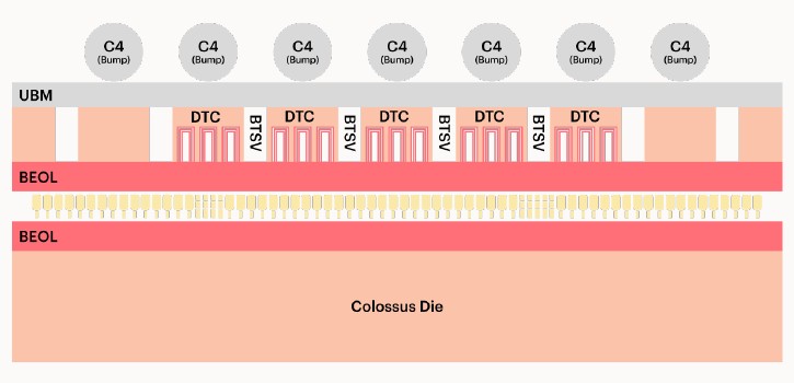
Yes, that die is inverted.
“Wafer on wafer is a more sophisticated technology,” explains Knowles, and he explains it best and clearly so we will let him do it for you as he did for us. “What it delivers is a much higher interconnect density between dies that are stacked on top of each other. As its name implies, it involves bonding wafers together before they are sawn. In the Bow IPU, we attach a second wafer to our processor wafer, and this second wafer carries a very large number of deep trench capacitor cells. This allows us to smooth the power delivery to the device, which in turn allows us to run the device faster and at lower voltage. So we get both higher performance and a better power efficiency. There are two enabling technologies behind wafer on wafer stacking. One is a type of bonding between two pieces of silicon from back end of line to back end of line. And you can think of this as a sort of cold weld between pads on the silicon devices. There are no interstitial bumps or anything like that. The second technology is a type of through silicon via called the backside through silicon via, or BTVS, and this allows power or signals to be connected through one of the wafers to the other. The effect of these two together is to deliver a very good power supply to the logic transistors on the logic die. This is just the first step for us. We have been working with TSMC to master this technology, and we use it initially to build a better power supply for our processor, but it will go much further than that in the near future.”
Incidentally, the power distribution wafer is bonded to the IPU wafer and then ground down to be very thin so the whole thing still fits into the Graphcore IPU package. This extra wafer is so thin that this is the only way you can do this, in fact. The Bow chip is made using a modified version of TSMC’s N7 7 nanometer process.
The net effect is that Graphcore can take its “Colossus” IPU running at 1.35 GHz, add the wafer-on-wafer power distribution to create the Bow IPU running at 1.85 GHz, and somewhere between 29 percent and 39 percent higher performance and burn 16 percent less power, too. Here is the distribution of performance increases on a variety of AI workloads:

The average performance gain is 36.3 percent across the 19 machine learning workloads shown above.
Here are the salient characteristics of the Bow IPU, which like Graphcore’s Poplar software development kit, is named after a neighborhood in London:

To be precise, the first and second Graphcore IPUs were named Colossus after the code-breaking machine created by Tommy Flowers in England during World War II. Poplar is the neighborhood where Flowers was born, and Graphcore is going to stick with London hoods for IPU codenames going forward.
The basics of the GraphCore IPU have not changed with the improved power. It still has 1,472 cores and 900 MB of in-processor SRAM memory, but now, with the higher clock speed engendered by better power distribution, the cores run 37 percent faster and the memory does to, yielding an aggregate of 65 TB/sec of bandwidth. The performance has risen to a proportional 350 teraflops, and that rating is based on 16-bit multiplication and 32-bit accumulation in floating point format; 32-bit floating point will yield one quarter of that, or 87.5 teraflops. But that is still 4.5X faster than the FP32 math on an Nvidia A100 GPU, according to Knowles.
Here are the feeds and speeds of the Bow-2000 system node using the Bow IPU:
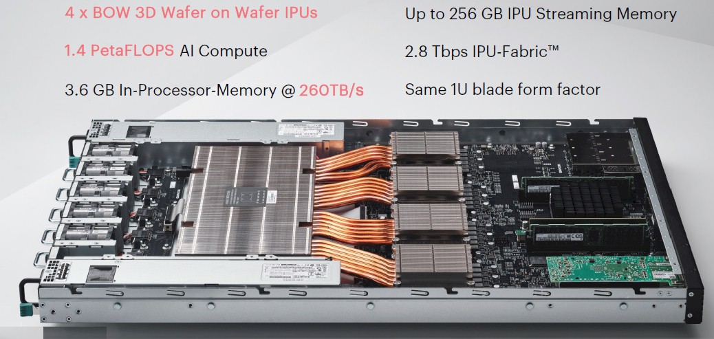
Each IPU has access to DDR4 “streaming memory” that can feed it data and that compliments the 900 MB of on-chip SRAM in-processor memory. The capacity of this streaming memory changes; it was 448 GB across four IPUs in the IPU-M2000 Classis nodes based on the second generation Colossus IPUs, and now it is down to 250 GB across the four IPUs with the Bow-2000 nodes. The host servers that drive these four IPUs can have up to 2 TB of main memory, also made from DDR4 chips.
The Bow-2000 nodes can be interlinked with the ten IPU-Link interconnect ports on each chip to spread work around a pretty decently sized cluster. Here is how the Bow machines can be podded up:
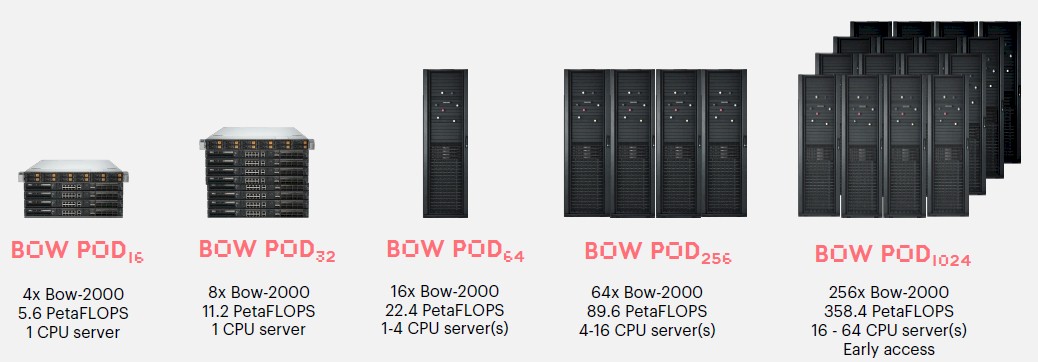
The Bow POD1024 would be a fun thing to play around with, eh? And if you have $9.5 million at list price discounted down to maybe, let’s call it a cool $7.5 million, you can play indeed.
Considering the performance advantage of the AI juggernaut that everyone is gunning for – that would be the Nvidia “Ampere” A100 GPU accelerator – you might want to run some benchmark tests on your AI workloads. Graphcore pit its Bow POD16 – and for some reason, we are digging the subscripts in the naming convention Graphcore, must be a chemical deficiency of some sort – with sixteen of its Bow IPUs against the DGX-A100 with eight A100s all linked by NVSwitch, doing a training run against the EfficeintNet-B4 neural network. Take a look:
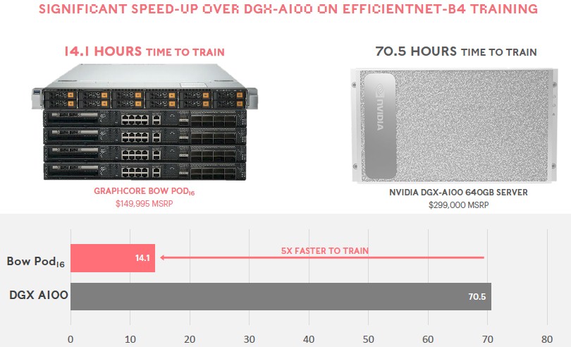
The Bow POD16 was able to train the model in 14.1 hours, precisely one-fifth of the time, and cost half as much. That is a factor of 10X better price/performance. We don’t know how much this gap will close with the A100 Next (sometimes called “Hopper”) GPU coming out from Nvidia, very likely in two weeks, but that won’t matter much if the demand is so high that you can’t get a Hopper GH100 or GH202 from Nvidia.
As usual, we would love to see how the new Bow machines fare on the MLPerf benchmarks. And we look forward to seeing such results because Graphcore, unlike many of its AI chip upstart peers, does run MLPerf tests on its iron.
Graphcore is providing that the Bow IPU at the same price as it was charging for the prior second-generation Colossus IPUs. Nigel Toon, the company chief executive officer, says that does not mean that Graphcore won’t lower price on the older IPUs, but it does mean that the extra performance is not coming at a higher initial cost. This is a good use for extra performance to drive more business instead of more revenue.
All of this brings us to the 10 exaflops “Good” machine that Graphcore is working on.
The Good in the machine name does not refer to the quality of engineering that Graphcore is bringing to bear, but rather refers to Irving John Good, a British mathematician who was a code-breaker along with Alan Turing at Bletchley Park. In 1965, he predicted that an “intelligence explosion” would happen in computing, and result in the fusing of human and machine intelligence as well as what he called “ultraintelligent machines,” which means exactly what it says: Machines that are smarter than us. And by the way, 33 years later, Good apparently predicted such a thing would cause an extinction event for the human species.
Toon and Knowles, as founders of Graphcore, want to build an ultraintelligent machine, and openly admit that this was their goal in creating the company. The human brain has around 100 billion neurons with somewhere on the order of 100 trillion synapses, which Toon says are roughly analogous to the parameters in an AI model. The largest models today, most of which run on GPU clusters, top out at around 1 trillion parameters.
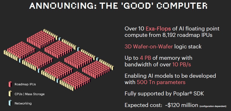
The Good machine, which may turn out to be used for good, evil, or both, is designed to be able to support 5X the number of parameters as the human brain has synapses, and that, says Toon, will require 8,192 of its future generation IPUs and over 10 exaflops of performance. (We presume that is 16-bit multiply, 32-bit accumulate, as in the metrics discussed above.) Such a machine will have over 4 PB of on chip memory and over 10 PB/sec of memory bandwidth across those IPUs. This system is anticipated to cost $120 million. Which is a lot more expensive than a human brain, but still a lot less expensive than an exascale-class FP64 math machine used to run HPC simulations or models, which costs about five times this amount based on a mix of CPUs and GPUs.
The Good machine, we have been assured, will definitely be able to play Crysis – and when we say play, we mean not run it for you, but run it as you, or better still, better than you.


Be the first to comment