

The modern GPU compute engine is a microcosm of the high performance computing datacenter at large. At every level of HPC – across systems in the datacenter, within clusters of disparate and diverse server nodes, within cluster nodes with disparate and diverse compute engines, and within each type of compute engine itself – there is a mix in the number and type of computing that is being done.
Thus, buying a supercomputer means trying to predict the mix of new and legacy workloads you will need over the next three to four years, possibly longer, and making sure you can run the old stuff and still take on the new stuff. And given the diversity of compute engines and the possible combinations of CPUs, GPUs, FPGAs, and custom ASICs, the number of possible combinations of performance at a given level or integer or floating point precision is staggering.
We would joke that you need an AI-infused HPC model, perhaps embedded in a crystal ball, to try to figure out what to buy – and in what capacities – but it is possibly not a joke. This is a really difficult proposition, and nothing makes this more apparent than trying to figure out how the new “Aldebaran” Instinct MI200 series of GPUs from AMD, announced last month, stack up against the “Ampere” A100 series of GPUs from Nvidia. But as we have pointed out before, whether they do it on the back of a drink napkin or in a complicated spreadsheet, customers building HPC and AI systems have to try to figure out what these devices cost on the street and what their key performance metrics are to reckon the value for the dollar systems built using them will deliver. And then they have to take into account the value of a mature software stack to make use of these devices, which is very difficult to quantify.
The Nvidia Ampere GPU accelerators aimed at the datacenter for big compute jobs and based on the GA100 GPU were announced back in May 2020, and the top-end A100 devices was enhanced with a fatter 80 GB HBM2e memory in November 2020. Nvidia has added a bunch of other accelerators based on the Ampere architecture since that time, including the Ampere A40 and A6000 accelerators in October 2020, based on the GA104 GPU, the Ampere A10 and A30 in April 2021, based on the GA102 and GA100 GPUs, respectively, and the Ampere A2 in November 2021, based on the GA107 GPU.
While there is always a chance that there will be more tweaks to the Ampere GPUs and different cards, we suspect that Nvidia will keep its powder dry publicly until the “Ampere Next” kickers to the A100 debut next year, right on time for their two year cadence very likely in March 2022 when GTC 2022 is hosted in San Jose. Everyone thinks that the Ampere Next GPU is also code-named “Hopper,” just to avoid confusion. We don’t know exactly what architectural changes will be made, but we are pretty sure Nvidia will do a process shrink to the 5 nanometer technologies at TSMC (N5 and N4 are possible, but the N4P process, a further 5 nanometer refinement, won’t be available until 2023). Nvidia will probably not push all the way down to 3 nanometer technologies (N3) with the Hopper GPUs, and that is because that N3 process has apparently had some issues.
No matter what, Nvidia will boost transistor counts and add lots of features with the Hopper GPUs. We strongly suspect that Nvidia will move to a chiplet architecture for the core GPU compute engines and will eventually move to 3D packaging technologies as well.
The point is this: The Aldebaran GPUs from AMD offer a substantial performance improvement over the current Ampere GA100 GPUs on a lot of metrics, but the Instinct MI210, MI250, and MI250X accelerators based on the Aldebaran GPUs are not yet shipping in volume to anyone except the US Department of Energy for the 1.5 exaflops “Frontier” supercomputer at Oak Ridge National Laboratory. And by the time AMD has the Instinct MI200s into the field in production, Hopper will be right around the corner in whatever Nvidia decides to call it.
But for the moment, the feeds and speeds of the Aldebaran GPUs make them a compelling alternative to Nvidia A100s – so long as you can make your code run on them, of course.
In briefings ahead of the Aldebaran launch a month ago, Brad McCredie, who used to run IBM’s Power processor development for many years before moving to AMD more than two years ago to become corporate vice president of GPU platforms, put together this chart that compares the peak double precision performance of Nvidia’s GPU accelerator cards that had 64-bit floating point performance – the “Maxwell” GPUs didn’t have much in the way of FP64, which is why the “Kepler” and “Pascal” and “Volta” and “Ampere” generations are only shown on this chart – over time.
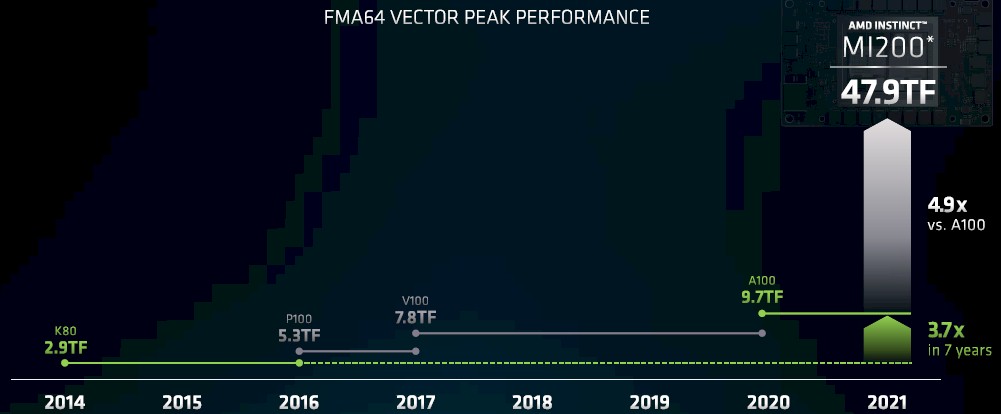
It is noteworthy that the prior generations of Instinct MI50, MI60, and MI100 GPU accelerators, based on the “Vega10” and Vego20” and “Arcturus” GPUs from AMD – are not shown on this chart above. But we walked through all the feeds and speeds here if you want to pencil them in. The Vega10 and Vega20 GPUs did not support matrix math units not mixed precision math below FP16 and did not support integer operations commonly used for machine learning inference. The MI60, which was supposed to be the top-end GPU a few years back, never really made it to market in any important way and AMD doesn’t talk about it much. With the Arcturus chip, AMD moved to the CDNA architecture, which focused solely on datacenter compute and did not give a card about graphics performance, and put a credible engine in the field that did FP64 and FP32 pretty well and added support for matrix math at FP64, FP32, FP16, and Bfloat16 formats.
With the Aldebaran GPUs, AMD created a GPU tile that supported all of the necessary vector and matrix units and in all of the appropriate precisions and formats, and then put two of these tiles on the Instinct MI200 series cards, with a double-whammy of Infinity Fabric links and HBM2e memory. And here is how McCredie stacked AMD’s Aldebaran to Nvidia’s A100:
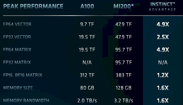
What is immediately obvious with the Aldebaran design is that AMD went all out on the FP64 vector processing, which is used for weather modeling and other kinds of physics simulations as well as machine learning training, as well as for FP32 vector processing, which is used for signal processing and genetics simulations, among other things. We think Nvidia could have thrown down a Hopper GPU that would have met these specs, but perhaps not at the price that the US government was willing to pay. IBM and Nvidia already sold two pre-exascale supercomputers to the Department of Energy, with “Summit” at Oak Ridge and “Sierra” at Lawrence Livermore National Laboratory, and did not seem keen on repeating that process at a low price, is our guess. They didn’t have anything to prove, but AMD did. And so Hewlett Packard Enterprise and Cray, working with AMD, boosted the performance by about 50 percent to 1.5 exaflops using a combination of AMD CPUs and GPUs and held the system price to the $500 million figure that IBM and Nvidia probably pitched with something just a hair over 1 exaflops.
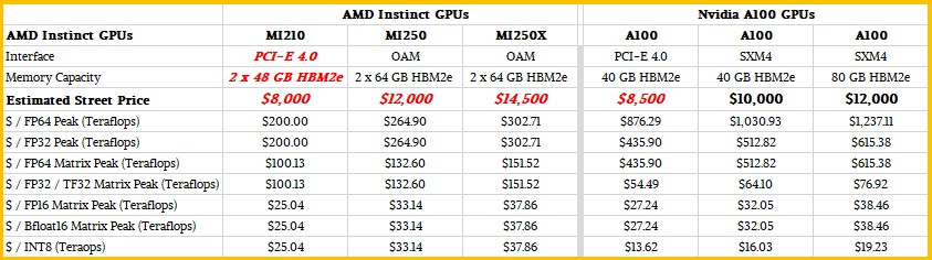
The A100 and the MI200 are not just two different accelerators that compete head to head, but two families of devices that have their own varying feeds, speeds, slots, watts, and prices. So this is a more complete table to show how the Aldebaran GPU accelerators stack up to the Ampere GPU accelerators:
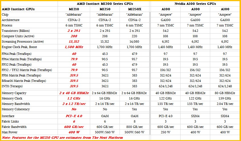
AMD has not said much about the PCI-Express variant of the Instinct cards based on the Aldebaran GPU, known as the Instinct MI210, so we took a stab at what it might be like. We assume that the clock speed is lowered and all of the compute units are active, but concede that it could have some more compute units idled through defects on the chips (to make the overall effective yield go up for the chips coming out of TSMC) and a higher clock speed. It could have both lower clock speed and fewer compute units and less HBM2e memory. You get the idea.
If Nvidia wanted to, Hopper could just be made with two A100s slapped down in a chiplet architecture, but that would not be enough to match the 4.9X FP64 vector and matrix performance advantage Aldebaran has, And, yes, Nvidia has the big advantage when it comes to mixed precision and number formats, especially if the applications are amenable to sparse matrix calculations (which AMD does not yet support). But for the core HPC customers, they need to do some inference or even a lot of inference, but they do not have to compete in the inference space with FPGAs or custom ASICs like Nvidia has to do with the whole idea behind the general purpose Ampere GA100 GPU for the datacenter.
It will be interesting to see exactly what Nvidia does, and it most certainly will be in anticipation of what AMD did to win the two of the three big exascale contracts in the United States with its Instinct GPU accelerators.
What matters, of course, is the performance of the MI200 versus the A100 on HPC benchmarks and real HPC applications. McCredie offered up this chart as food for thought:
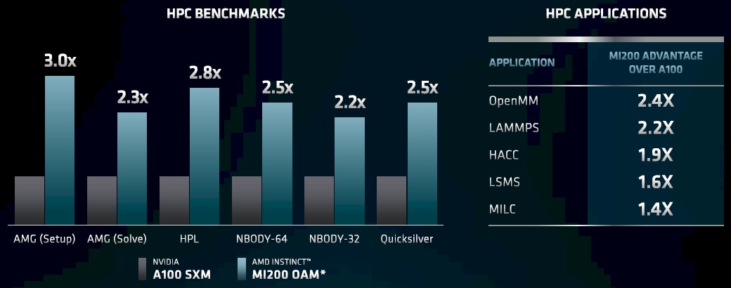
As you can see, the performance numbers are definitely in favor of the Aldebaran GPUs, each half of which has a little bit more performance of the whole A100 on common HPC benchmarks and a little less than that on the HPC applications shown on the right part of this table. The gap is not as big as raw feeds and speeds show, and we think that has to do with the maturity of the compilers and math libraries in the ROCm stack from AMD for its own GPUs versus the CUDA stack from Nvidia for its own GPUs. There is $100 million in non-recurring engineering funds in the Frontier system alone to try to close some of that ROCm-CUDA gap.
And what really matters is the bang for the buck of the devices, and so we have taken the Nvidia A100 street prices, shown in black, and then made estimates shown in red. The estimates for pricing for the AMD MI200 series GPU accelerators are what we think are balanced prices that give very good competitive advantage on FP64 and FP32 workloads common in HPC and then respectable bang for the buck on the mixed precision stuff.
As a check against our hunches we did this little thought experiment. Assuming about a $5,000 a pop price tag for the custom 64-core “Rome” processor in Frontier, and assuming that 20 percent of the $500 million cost of the total machine was for Slingshot network, disk storage, and the Shasta enclosures, and 15 percent was for main memory, what price would it have to be to make the CPU and GPU costs be about two-thirds of the overall cost of the machine? The answer for the Instinct MI250X is $8,000. If you do some rough math backwards, the V100 GPU accelerators used in the Summit supercomputer listed for around $7,500 and sold for around $4,000 in the system. Assuming the same level of discounting that Nvidia might have given on the GPUs, then the MI250X should cost around $14,500 at list price.
If you make all of those assumptions, then here is how the two families of GPUs stack up with regards to bang for the buck on peak theoretical performance metrics:
And what really, really matters is the value for the dollar on real world workloads, but we will have to wait until there are real prices and real benchmarks before we can get into that. Enough extrapolating dangerously for the day. Suffice it to say, if the performance gap is not as big on real benchmarks and real workloads, then the price/performance gap can’t be as big, either. But a lot depends on pricing, and those can be changed on a whim before AMD has volume shipments of the MI200s next year.


Can AMD Keep Doubling Its Datacenter Business?
Imagine, if you will, that AMD could make as many Epyc CPUs and Instinct GPU accelerators as it wanted at a reasonable yield and cost. How much larger would its datacenter business already be, setting aside the $49 billion acquisition of FPGA maker Xilinx, completed earlier this year, and the …
Intel’s First Discrete Xe Server GPU Aimed At Hyperscalers
We have been waiting for years to see the first discrete Xe GPU from Intel that is aimed at the datacenter, and as it turns out, the first one is not the heavy compute engine we have been anticipating, but rather a souped up version of the Iris Xe LP …
Spectrum-4 Ethernet Leaps To 800G With Nvidia Circuits
When Nvidia announced a deal to buy Mellanox Technologies for $6.9 billion in March 2019, everyone spent a lot of time thinking about the synergies between the two companies and how networking was going to become an increasingly important part of the distributed systems that run HPC and AI workloads. …
I am no expert, but there seem some some astonishing ~”dont u worry about that” pontifications here.
” We strongly suspect that Nvidia will move to a chiplet architecture” – excuse me?
We are not talking some new fashion which can chosen & implemented on a whim.
Chiplets and vitally, Infinity Fabric, has been incubated, patented & validated since the early 2000s
It treats 2TB/s vs amd’s 3TB/s bandwidth as if they are like metrics which is absurd
One is a measure of a gpu onboard local bus. The other, the Infinity Fabric speed that can connect cores & cache on multi gpuS. Nvidia must revert to the snail’s pace of pcie for this.
Nvidia have very little say in the host’s ecosystem, unlike amd’s total control over co-developed cpu/gpu/platform ecosystems.
NVIDIA has been incubating, patenting, and validating chiplets for years, as well. It is an industry-standard direction of moment. That’s well-known. It should not at all be controversial to say they strongly suspect NVIDIA will be moving to a chiplet architecture. The only thing is they likely won’t call them chiplets. In their research they seem to call them multi-chip modules, for example, this paper from 4 1/2 years ago: https://research.nvidia.com/publication/2017-06_MCM-GPU%3A-Multi-Chip-Module-GPUs
I’m not sure why you are claiming NVIDIA must use PCI-E to connect multiple GPUs when they have had NVLink for years. And their ability to do that with x86 CPUs is not a matter of technical ability but a matter of their competition with the x86 chip manufacturers meaning those manufacturers will not allow the technology on their chips. Finally you seem to be under the impression that AMD achieves its aggregate memory bandwidth of 3 TB/s across its infinity fabric, which has a bandwidth of 800 GB/s. I don’t understand that assertion at all.
Regarding NVIDIA’s access to the host memory and cache that should change in 2023 with Grace for supercomputers and perhaps CXL in data center, although it’s unclear to me whether the 2.0 or 3.0 specification will be when it is introduced in the data center.
Although the Mi250X uses 2 dies, they are quite small in comparison to an A100 and only use 7% more transistors overall. The fact that AMD have been able to out perform the a100, to a great extent in certain tasks over 2x, with only 7% more transistors is nothing short of a marvel, they’ve literally came from pretty much no ground in the data centre, to after just 2 generations of CDNA, they’re competing with their competitors top products.
Arcturus (CDNA-1) has 25.6B transistors in 750 square mm on TSMC 7 while GA100 has 54.2B transistors in 826 square mm on TSMC 7. So NVIDIA has a much higher areal density of transistors than both CDNA-1 or CDNA-2. I won’t venture to guess why that is, but it is die area that’s the important scaling factor to look at, not the number of transistors.
As far as AMD’s ability to outperform the A100, it must be said that Aldebaran is a next generation part when compared to the A100 and those performance data are from supercomputing applications. Aldebaran is a part that caters to the supercomputer market while the A100 is not. It would be interesting to see Aldebaran’s performance in the areas where NVIDIA is commercially targeting their processors these days.