
UPDATE: One of the reasons why Intel spent $16.7 billion to acquire FPGA maker Altera six years ago was because it was convinced that its onload model — where big parts of the storage and networking stack were running on CPUs — was going to go out of favor and that companies would want to offload this work to network interface cards with lots of their own much cheaper and much more energy efficient processing.
This is what we used to call SmartNICs, which meant offloading and accelerating certain functions using a custom ASIC on the network interface card. We are now increasingly calling them DPUs, short for Data Processing Units, as these devices get a hybrid approach for their compute and acceleration, mixing CPUs, GPUs, and FPGAs together on the same device. Because it has to be different, Intel gives offload devices that are substantially expanded SmartNICs the name Infrastructure Processing Unit, or IPU — but to avoid confusion we are sticking with the DPU name for all of these.
In any event, Intel trotted out three of its impending DPUs at its recent Architecture Day extravaganza, and the executives in its Data Platforms Group showed that they had indeed been on the road to Damascus for the past couple of years and were going to not only stop persecuting DPUs, but embrace them fully. Well, it was not so much a conversion as it was an injection of new people bringing new thoughts, and this includes Guido Appenzeller, who is these days chief technology officer at what used to be called the Data Center Group. Appenzeller ran the Clean Slate Lab at Stanford University, which gave birth to the OpenFlow software defined networking control plan standard and was co-founder and CEO of at Big Switch Networks (now part of Arista Networks). Appenzeller was chief technology strategy officer at the Networking and Security business unit at VMware for a while and was behind the OpenSwitch open source network operating system project created by Hewlett Packard Enterprise a few years ago.
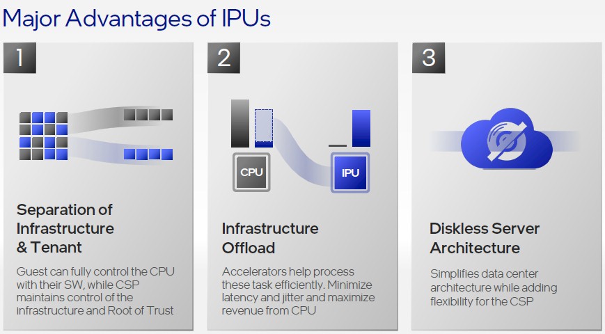
Intel has not talked much about offloading work from CPUs, because that is heresy — even if it is happening and even if there are very good economic and security reasons for doing so. The metaphor for DPUs that Appenzeller came up with, and talked about at Architecture Day, is clever. It’s more about resource sharing and multitenancy than it is getting better price/performance across a cluster of systems, which we think is the real driver behind the DPU. (This is hairsplitting, we realize. Offloading network and storage to the DPU helps cut latency, helps improve throughput, lowers cost, and delivers secure multitenancy.)
“If you want to think about an analogy, this is a little bit like hotels versus single family homes,” explained Appenzeller. “In my home, I want it to be easy to move around from the living room to the kitchen to the dinner table. In a hotel, it is very different. The guest rooms and the dining hall and the kitchen are cleanly separated. The areas where the hotel staff works is different from the area where the hotel guests are. And you get a bed, you may want to move from one to the other in some cases. And essentially this is the same trend that we’re seeing in cloud infrastructure today.”
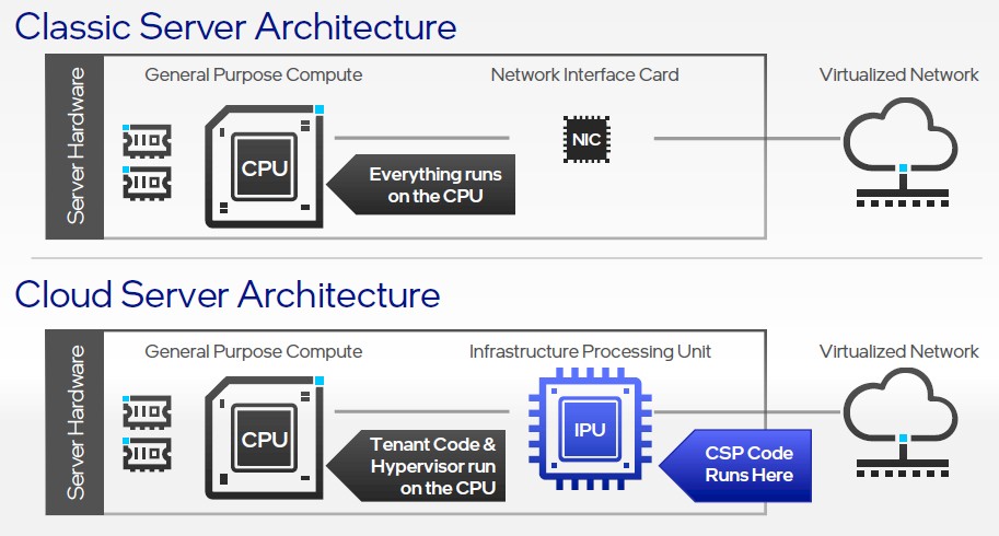
In the Intel conception of the DPU, the IPU is where the control plane of the cloud service providers — what we call hyperscalers and cloud builders — runs and the hypervisor and the tenant code runs on the CPU cores inside the server chassis where the DPU is plugged in. Many would argue with this approach, and Amazon Web Services, which has perfected the art of the DPU with its “Nitro” intelligent NICs, would be the first to raise an objection. All network and storage virtualization code runs on the Nitro DPU for all EC2 instances and, importantly, so does the server virtualization hypervisor excepting all but the very tiniest piece of paravirtualized code that has nearly no overhead at all. The CPU cores are meant only to run operating systems and do compute tasks. No more.
In a sense, as we have been saying for some time, a CPU is really a serial compute accelerator for the DPU. And not too far into the future, the DPU will have all accelerators linking to it in a high-speed fabric that allows the whole shebang to be disaggregated and composable, with the DPU — not the CPU — at the heart of the architecture. This is going too far for Intel, we suspect. But this makes more sense, and fulfills a lot of the four-decade vision of “the network is the computer” espoused by former Sun Microsystems techie extraordinaire John Gage. There will be more and more in-network processing, in DPUs and in switches themselves, as we move forward because this is the natural place for collective operations to run. Perhaps they never should have been put on the CPU in the first place.
To be fair, later in his talk, as you see in the chart above, Appenzeller did concede that CPU offload is happening, allowing customers to “maximize revenues from CPUs”. Intel surely has been doing that for the past decade, but that strategy no longer works. Which is one of the reasons why Appenzeller was brought in from outside of Intel.
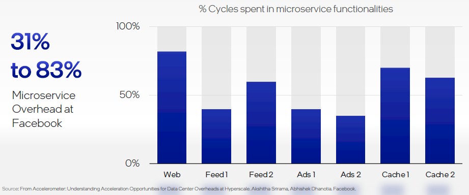
And this data below, from Facebook, that Appenzeller cited makes it clear why Intel has had a change in thinking — particularly after watching AWS and Microsoft fully embrace DPUs over the past several years and other hyperscalers and cloud builders following suit with various levels of deployment and success.
This is perhaps a generous dataset — particularly if you are not including the overhead of a server virtualization hypervisor, as many large enterprises have to even if the hyperscalers and cloud builders tend to run bare metal with containers on top.
At the moment, because it does not have its oneAPI software stack fully cooked and it does not have an ecosystem of software running on GPU-accelerated devices, Intel is only talking about DPUs that are based on GPUs, FPGAs, and custom ASICs. But in the fullness of time, we believe that GPUs, which excel at certain kinds of parallel processing and are faster to reprogram than FPGAs, will be part of the DPU mix at Intel, as they have come to dominate at Nvidia. It’s only a matter of time.
For now, two of the DPUs that Intel showed off at Architecture Day were based on CPU and FPGA combos — one called “Arrow Creek” that is based on an FPGA/CPU SoC, one called “Oak Springs Canyon” with a mix of an FPGA plus an external Xeon D processor — or was based on a custom ASIC code-named “Mount Evans” that Intel was creating for a “top cloud provider” that remains unnamed.
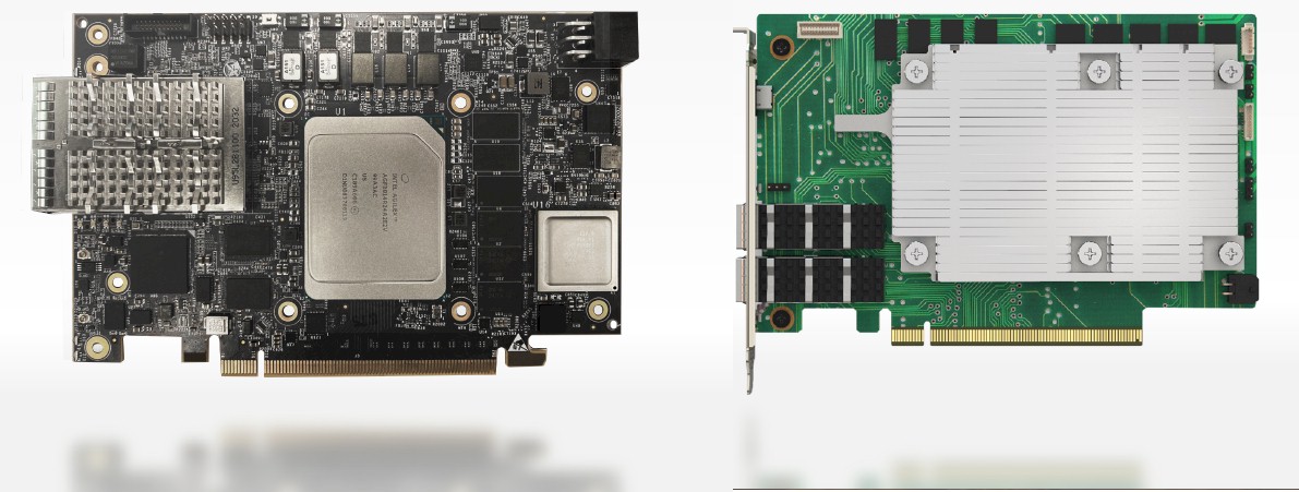
Here are the Arrow Creek (left) and Oak Springs Canyon (right) cards, which plug into PCI-Express slots inside of servers:
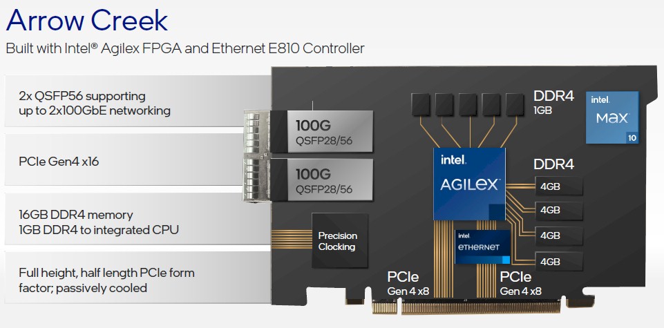
And here is a drilldown on Arrow Creek’s features:
The Arrow Creek DPU has two 100Gb/sec ports that use QSFP28 connectors and has an Agilex FPA compute engine. The DPU has a dual-port E810 Ethernet controller chip that hooks into eight lanes of PCI-Express 4.0 slot capacity and the Agilex FPGA has its own eight lanes of PCI-Express as well; both run back into the CPU complex on the servers through the PCI-Express bus. The Agilex FPGA has Arm cores embedded on it, and these can run modest compute jobs and have five channels of memory (four plus a spare it looks like) with a total of 1GB of capacity. The FPGA part of the Agilex device has four channels of DDR4 memory with a combined 16GB of capacity.
This Arrow Creek DPU is aimed specifically at network acceleration workloads, including customizable packet processing done on “the bump in the wire” as we have been saying about FPGA-accelerated SmartNICs for a long time. This device is programmable through the OFS and DPDK software development kits and have Open vSwitch and Juniper Contrail virtual switching as well as SRv6 and vFW stacks already shaped onto their FPGA logic gates. This is for workloads that change sometimes, but not very often, which is what we have been saying about FPGAs from the beginning.
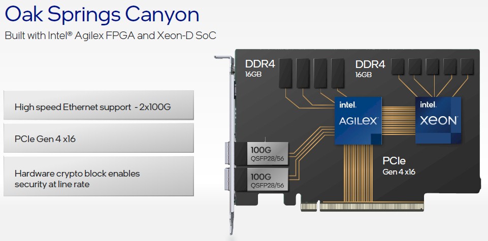
Oak Springs Canyon is a little different, as you can see:
The feeds and speeds on the Xeon D processor were not revealed as yet, but it probably has 16 cores as a lot of SmartNICs tend to these days. As far as we know, the Xeon D CPU and Agilex FPGA are on the same die — Intel has been working on this for years and promised such devices as part of the Altera acquisition back in 2015 — but for all we know they are integrated in a single socket using EMIB interconnects. The CPU and GPU each have 16GB of DDR4 memory across four channels, and they link through the FPGA to a pair of 100Gb/sec QSFP28 ports.
The Oak Springs Canyon DPU is programmable through the OFS, DPDK, and SPDK toolkits and have integrated stacks for Open vSwitch virtual switching as well as the NVM-Express over Fabrics and RoCE RDMA protocols. Obviously, this DPU is aimed at accelerating network and storage and offloading it from the CPU complex in the servers.
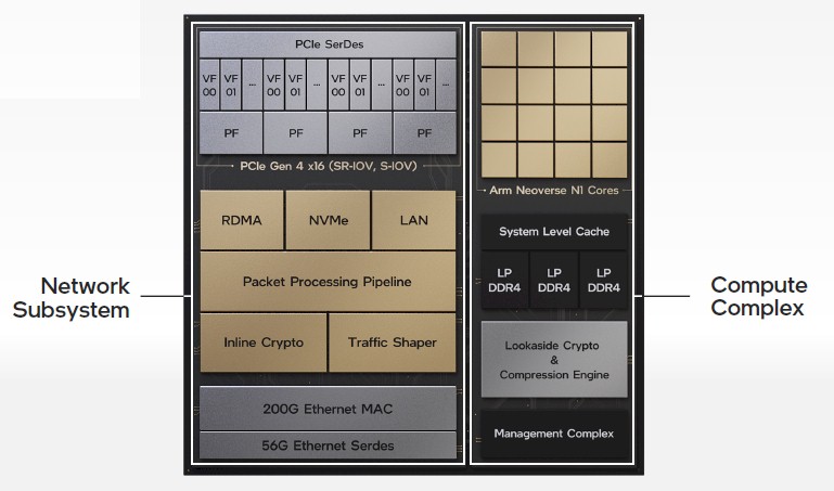
The third DPU, the Mount Evans device, is perhaps the most interesting in that it was co-designed with that “top cloud provider” and that it has a custom Arm processor complex and a custom network subsystem integrated on the same package. Like this:
The networking subsystem has four SerDes running at 56Gb/sec, which delivers 200Gb/sec at full duplex and which can be carved up and used by four host servers. (The charts say it has to be Xeons, but it seems unlikely that this is a requirement. Ethernet is Ethernet.) The network interface implements the RoCE v2 protocol for accelerating network without involving the CPU (as RDMA implementations do) and also has an NVM-Express offload engine so the CPUs in the host don’t have to deal with this overhead, either. There is a custom programmable packet processing engine, which used the P4 programming language and which we strongly suspect is based on chunks of the “Tofino” switch ASICs from Intel’s acquisition of Barefoot Networks more than two years ago. The network subsystem has a traffic-shaping logic block to boost performance and lower latency between the network and the hosts, and there is also a logic block that does IPSec inline encryption and decryption at line rate.
The compute complex on the Mount Evans device has 16 Neoverse N1 cores licensed from Arm Holdings, which are front-ended by a cache hierarchy that was not divulged and an unusual three DDR4 memory controllers (that’s not a very base-2 number). The compute complex also has a lookaside cryptography engine and a compression engine, thus offloading these two jobs from the host CPUs, and a management complex to allow outboard management of the DPU.
It is not clear what the workload is, but Intel says that as for the programming environment, it will “leverage and extend” the DPK and SPDK tools, presumably with P4. We strongly suspect that Mount Evans is being used in Facebook microservers, but that is just a guess. It could be Google, and it definitely is not AWS or Microsoft. And we also strongly suspected that it would not available to anyone other than its intended customer, which we said when this story first came out would be a shame.
Update: Intel apparently will commercialize Mount Evans. At some point.
Here is the statement we got from Brian Neipoky, director of Connectivity Group Marketing at Intel, after the story ran: “Mount Evans will be commercially available, but we are not announcing product availability at this time.”
So, there is a little more precision, and you are welcome.


Be the first to comment