The package is the most compact platform to do heterogenous integration for IP that can’t be naturally integrated in silicon but steady incremental improvements versus game-changing approaches are the only foreseeable path forward.
Advanced packaging technology is often not at the top of the list of stories around top chipmakers but Intel is making it a point to define the area as one of the keys to helping the company stave off the pressing impacts of Moore’s Law.
This push to emphasize the role of packaging is all for good reason, pushing innovation at the component level can lead to increased heterogeneity, connectivity, and bandwidth while lowering power consumption. This is an area where Intel has consistently pushed the envelope harder than others, the problem is we don’t tend to hear much about it.
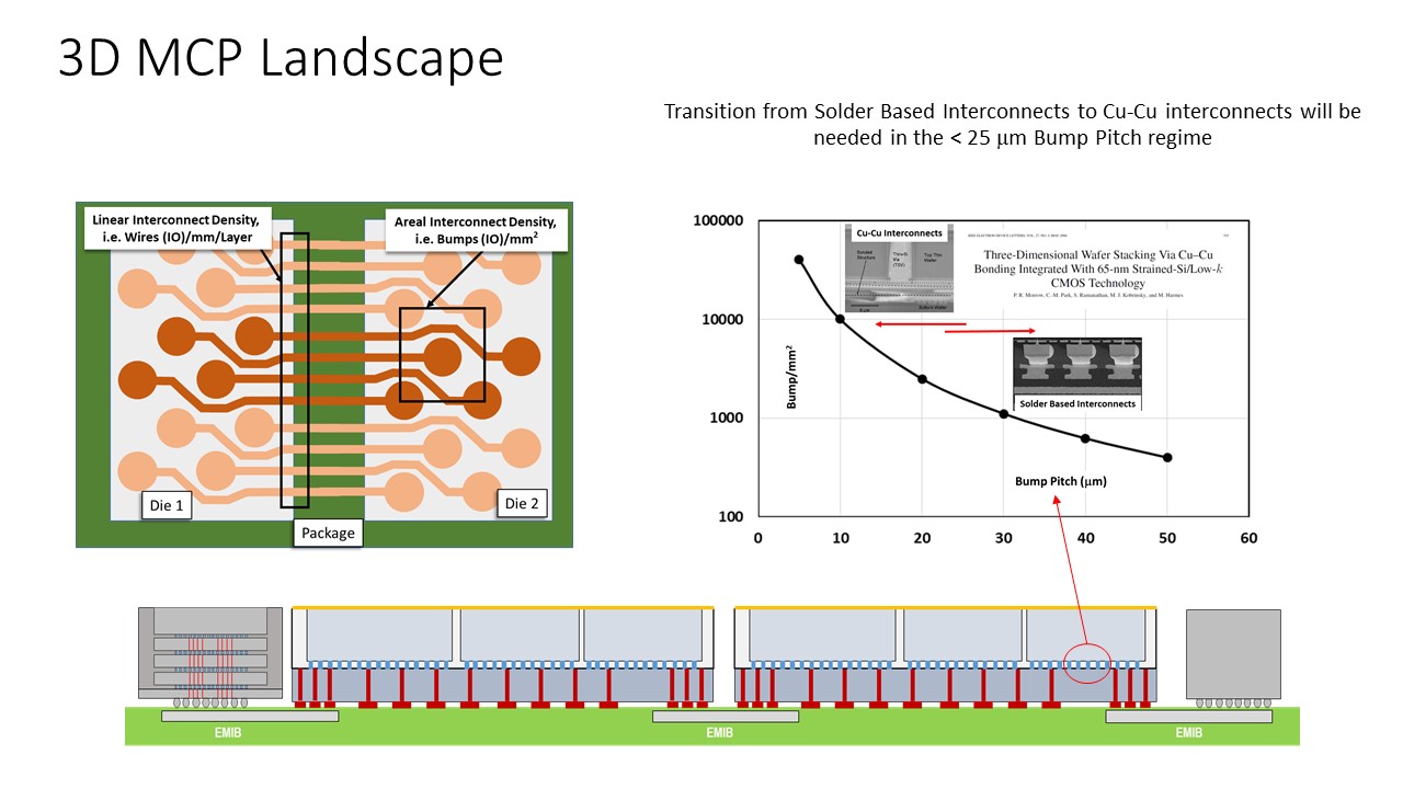
In the last decade-plus, Intel has developed a number of technologies to keep pace with both economic and technical challenges—issues that will be more pronounced over the next several years. Many of the most important developments are at the interconnect level. If we look at technologies in this sphere Intel has developed, there are options for everything. For instance, there is EMIB, which has been around for over a decade and allows for localized connections. For high-density connections, they can also reel in silicon interposers. And with technologies like Foveros they can also do stacking with the added ability to have 3D and 2D that can be stitched together to create scale-up and scale-out architectures, not to mention the capability for omni-directional interconnects.
In this span too, the chip industry overall has made several critical pivots. From wire-board to aerial interconnects; from ceramic to copper/organic; the transition from lead-baed to lead-free solder; from pin-grid to line-grid. All of these broader technologies were developed while Ravi Mahajan was at Intel, first on the thermomechanics side before moving into interconnects in 2000, just in time for another important shift—one that pushed Intel to develop EMIB in the early 2000s: the shift from a serial worldview to one focused on parallel lanes. This opened the door to the kinds of high-density interconnects we have today.
Now, as Intel Fellow in the Pathfinding group, Mahajan is looking ahead at the possibilities and limitations at the component level and via work with DARPA, DoD, and other groups who want to understand the future of the systems that will require increasingly high performance and efficient devices. For Mahajan, the parallel path is one that is known, but will get rockier. “There’s been a lot of thought put into the wide and slow parallel versus serial question. One limiter in parallel links is that we need complex packaging and have to worry about yield and cost. But if you get this all to work together you can deliver high bandwidth, lower latency interconnects between die with lower power,” Mahajan says.
What’s interesting is that the challenges of high density then only have become more pressing in the heterogenous era, namely the integration balancing act. Getting ultimate power efficiency and performance with increasingly more happening on a device is not simple to begin with and while Mahajan says there are promising technologies on the horizon, he can only see to 2050 on the product spectrum.
Some have made the argument that 5nm might be the end of the road. The optimists say 3nm. Mahajan is definitely in the optimistic camp.
“If you say the focus of these interconnects is to double in bandwidth every generation, we’re still between generation one and two of that. We have at least three more generations and conceptually, each of these can last two to three years. That gives us at least 10-15 more years.” Product-wise, he adds, “we won’t run out of gas until 2060. Even then, we may run out in bit scaling but not in scaling features—we can keep adding Lego blocks and building more complex structures, assuming yield is under control.”
“In the big picture view, we have different IP implemented and optimized on different silicon processes and stitched together in the package. That end result must perform as close to an SoC as possible. We’re focused on figuring out how to develop the interconnects that connect these chips on a package in a compact way that can be cooled with clean power delivery and that on-package interconnect between components and the interconnect leaving the package can’t restrict performance.”

Getting to this 2050 (or 2030, for that matter) is a matter of incremental steps in technical areas including thermal management and power delivery but cost will ultimately preside.
“In terms of thermals, we will have to pay exquisite attention to make sure we can manage continued progress. You bring different types of die, maintain their temperatures at the optimal level and integrate, bring them closer. We can improve materials and look at how to spread the heat and take it away,” Mahajan says when asked what R&D promise there is on the horizon. Also, with all the different die’s power delivery networks being pulled together there will need to be more intelligent design of these architectures, he adds.
This 2050 extended timeline means all of the above innovations without sacrificing performance or communication or cost. Oh, cost. How can Intel (or other chipmakers) keep scaling with this heaviest of limitations?
“It’s hard to project,” Mahajan says. “But the way Intel has done business is to improve yield and take incremental steps to keep increasing density. It’s hard to predict when we’ll run out of economic gas or infrastructure but we’ve seen sufficient work to tell us we still have a lot of room to play.” He adds that the focus is on yield and scale.
“If scale gives cost advantage and yield lets you work better, those are two things that will keep moving us forward. We can contain cost by focusing on engineering. But technology will have more legs than cost.”


Be the first to comment