
For about a decade, Intel has sold GPUs, in recent years with its integrated CPU-GPU devices used in client and entry servers. But for the most part, at its heart and despite acquisitions of FPGA and NNP makers, Intel is still a CPU maker.
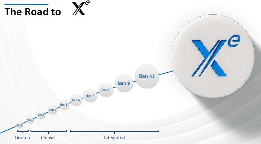
Nvidia and AMD have for years taken the lead on GPU development and sales, with Intel assuming more of a back seat. The massive chip maker hasn’t been sitting idle – Intel’s got 11 generations of its GPU technology under its belt – but the integrated offerings haven’t always measured up to the products put out by its competitors.
That said, Intel over the past couple of years has expanded its GPU ambitions and has pushed those efforts further into the spotlight. At an Intel Architecture Day event two years ago, David Blythe, Intel Fellow and chief GPU architect, introduced the company’s Xe initiative to build integrated and discrete GPUs for a range of workloads, from laptops and gaming systems to datacenter and HPC systems. The plan is to become a complete GPU vendor that will rival Nvidia and AMD.
Intel in the past several months have started to offer more information about the strategy at event such as the latest Intel Architecture Day in August and, most recently, the virtual Hot Chips 2020 conference later in the month, where the chip maker’s focus was on the Xe architecture and giving hints about other details that are yet to come. During his keynote at Hot Chips, Raja Koduri, the company’s chief architect, vice president, and general manager of the Cores and Visual Computing and Edge Computing Solutions unit, put a focus on the GPU strategy when talking about the need to address the massive amounts of data being generated by the billions of intelligent devices connecting to networks and the growing demand for artificial intelligence (technologies that is needed to help analyze all that data.
The industry will continue to see information about the Xe technology come out. The latest “Tiger Lake” CPUs that are expected to launch his week will include integrated Xe GPUs, with reports saying that the Iris Xe GPU will offer a clock speed of 1.65 GHz, helping the Tiger Lake CPU come in at twice the performance of its “Ice Lake” predecessor.
At the Hot Chips event, Blythe gave a look at some of the key aspects of the Xe architecture that make it significantly different from the previous generations of Intel GPU technology and part of a larger strategy to become a key GPU vendor.
“In our current work, we have embarked on a significant advancement in architecture and in our ambitions to encompass a much broader product space than previously covered by our integrated GPU architecture,” he said. “To mark that change, we made a change in the architecture naming from Gen to Xe. Xe has its roots in the phrase ‘exascale for everyone.’ Xe has some pretty ambitious goals. One, increase the scalability of the GPU from hundreds of SIMD lanes to many thousands. Next, provide great feature configurability to support SKUs for different workload specializations – media, 3D, AI, HPC and others. Next, add additional features beyond those in the previous Gen 11 architecture: matrix tensor processing, reliability, availability and serviceability features, ray tracing, virtualization and others. And last but not least, significant performance, power and area improvements compared with the previous generation.”
Blythe added that “meeting these goals was a major undertaking by the team and required a substantial amount of new architecture design to move beyond the great work the team had previously done on job.”
The Xe Lineup
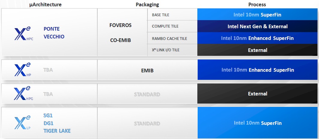
Intel is creating a single GPU architecture that can address a broad array of compute demands through four different microarchitectures. Xe HPC is aimed at exascale-level workloads and HPC clusters – including the “Aurora” A21 supercomputer, which will deployed at the Argonne National Lab next year and will include 7 nanometer “Ponte Vecchio” GPUs – Xe HP for datacenters, AI workloads and enthusiast segments, Xe HPG for the mid-market and gaming arenas, and Xe LP for entry-level environments for both integrated and discrete GPUs.
The microarchitectures will come over time, led by the Xe LP offering, which will begin appearing in the Tiger Lake processors. Xe HPC is due out next year, while both the Xe HPG and HP are being developed in the labs with no announced release dates. The microarchitectures come with various features as shown below that will optimize their capabilities for their targeted market segments, from a single slice design for Xe LP to multiple tiles and HBM2e memory for both Xe HP and HPC:
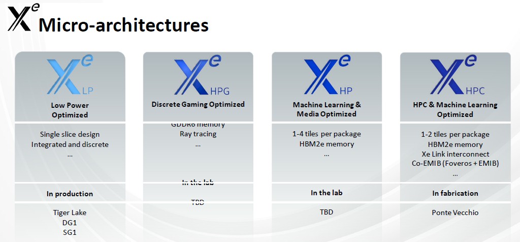
“One aspect we noticed is that there is both a desire and an opportunity to create more customized views,” Blythe said. “They’re cost- and performance-optimized for different market segments. What I mean by that is not just scale the number of shader units up and down, but independently modulate other capabilities and throughputs. A simple and traditional example is floating point 64 [FP64] throughput. It’s super-important in some markets and [in] others, it just takes up space area leakage. Other examples are 3D fixed function, matrix processing, display, media processing [and] ray tracing.”
The Xe GPU Architecture
At a high level, the architecture drives scalability through modular building blocks that are replicated and interconnected via high-bandwidth data buses, which Intel calls 3D compute slices. Within these slices are the elements for programmable processing, including 3D fixed-function support, media slices for video encode and decode and video processing, and the cache interconnect fabric.
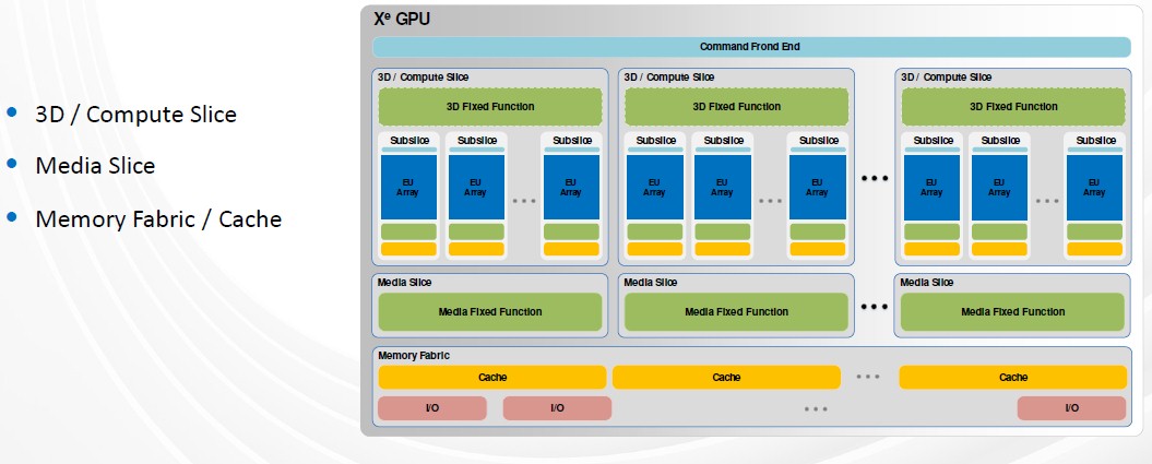
“The slices are further partitioned into a set of sub-slices,” he said. “These group programmable shaders we call execution units, with fixed-function logic that together naturally scale through replication. These sub-slices are combined with additional geometry and pixel processing functions, slice common, that are statically provision for optimum slice size. The slice sub-size partitioning has been present through multiple generations of Intel GPU architecture going back to at least Haswell integrated, or Gen 7.5, but many details have changed from generation to generation to our new capabilities, improved scaling and so on.”
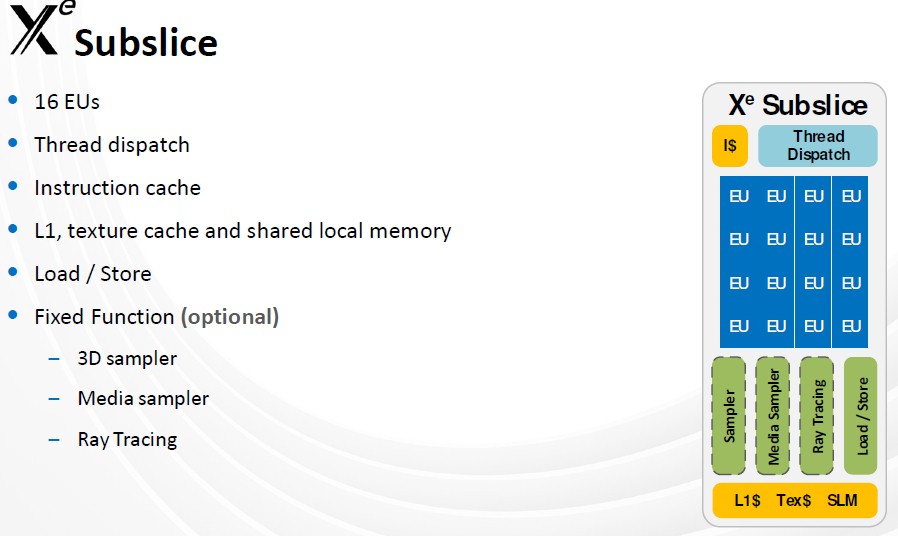
A key change Intel made was moving geometry processing from outside to inside the slice and having it work in a distributed fashion. Slice size also is key, he said, adding that “for large systems in a really large area, bigger is better, but for smaller systems in more confined spaces, smaller is better. In Xe, we’ve continued to maintain elasticity in the slice size. Elasticity comes from modulating the number of sub-slices.”
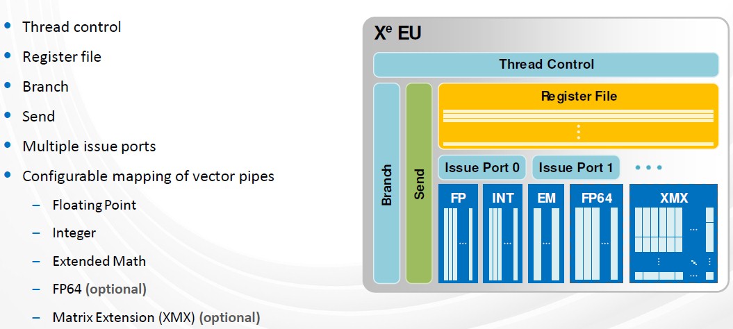
To improve area and power efficiency while growing configuration sizes, the number of execution units in the sub-slices in the Xe architecture increased from eight to 16, so the slice configurability is in multiples of 16 execution units or 128 SIMD lanes. Below is a look at the execution unit:
Xe Memory Fabric
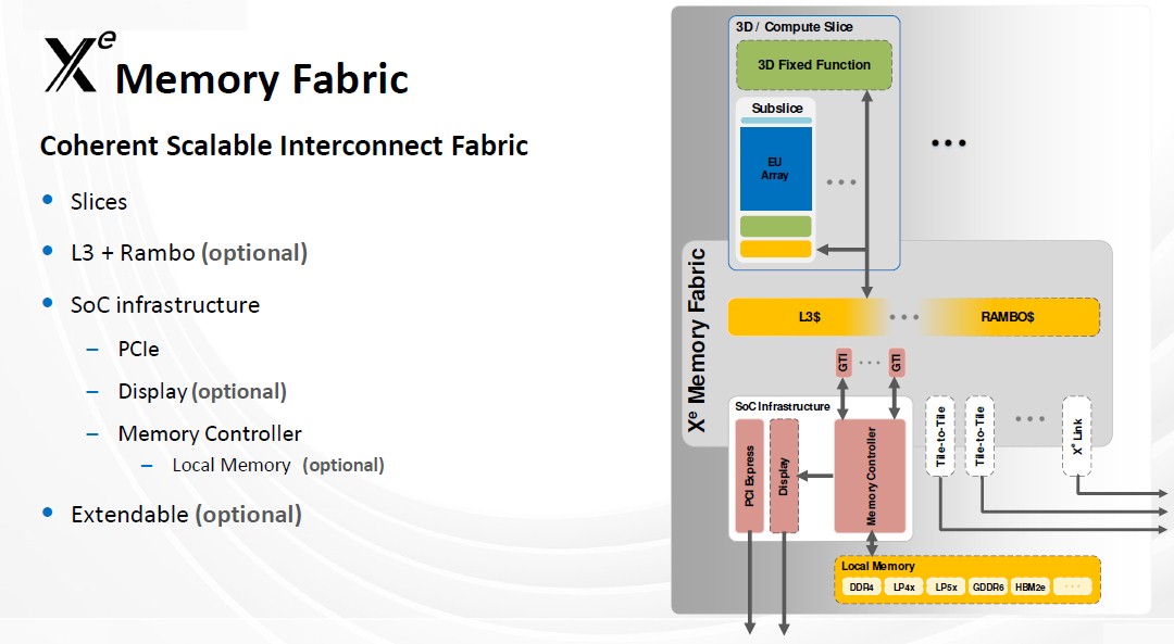
Foundational to the architecture is the XEMF [Xe Memory Fabric], a coherent, scalable memory fabric that interconnects the computing and media slices, the L3 cache and external memory subsystem. The fabric scales with a number of slices and the number of cash banks also scales with the fabric. The fabric is configurable based on the number of slices and ports of channels to the external memory subsystem. It also includes advanced packaging technologies, including Intel’s Foveros 3D stacking to connect the pieces together, and parts of the cache can be implemented in another die to create a significantly larger cache. Blythe said the “disaggregated cache is something we’re implementing as part of the Ponte Vecchio design. The external memory system connects to the Xe Memory Fabric through an adapter … that supports both integrated and discrete graphics.”
For integrated graphics systems like Tiger Lake, the adapter connects directly to the SSD internal high-bandwidth infrastructure. In discrete GPUs, there’s a separate scalable memory substystem that’s part of the SoC infrastructure, along with the PCIe display. That memory subsystem supports a range of memory technologies, from GDDR to high-bandwidth memory, Blythe said.
The Xe HP and HPC designs use multiple tiles that can work as individual GPUs or a single GPU. The Xe Link technology enables XEMF to run between GPUs. It’s currently running in GPUs in Intel labs.
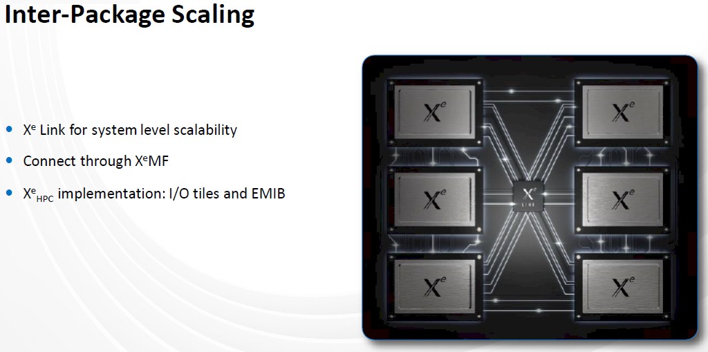
“While we know the inter-package scaling allows designs and more than 1,000 execution units, we also know that the computational demands for supercomputing applications or deep learning training require scaling even further,” he said. “The Xe architecture allows a hub with inter-package links to also connect at the node in the XEMF fabric.”


Will Open Compute Backing Drive SIOV Adoption?
Virtualization has been an engine of efficiency in the IT industry over the past two decades, decoupling workloads from the underlying hardware and thus allowing multiple workloads to be consolidated into a single physical system as well as moved around relatively easily with live migration of virtual machines. It is …
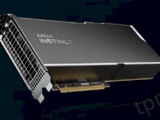
AMD Rounds Out “Aldebaran” GPU Lineup With Instinct MI210
When the “Aldebaran” datacenter GPUs were launched by AMD last November for the HPC and AI crowd pushing up into the exascale stratosphere, only the two top-end models of the Instinct GPU accelerators –ones that use the Open Accelerator Module (OAM) form factor put forth by Facebook and Microsoft under …
Being Persistent With Persistent Memory
Intel in October clarified its memory plans moving forward when it announced it is selling its NAND memory business to SK Hynix in a two-step acquisition that is worth $9 billion and will take until 2025 to be completed. However, while the deal itself is unusual – the deal is …
On the GPU connecting to “SSD internal high-bandwidth infrastructure” ,,,
What are the implications of this? Are you saying it is on the PCIE4 bus?
Is this something significantly different than the gen11 GPU connection on Ice Lake?