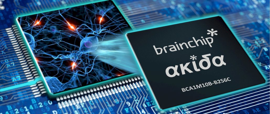
Neuromorphic computing has garnered a lot of attention over the past few years, largely driven by its potential to deliver low-power artificial intelligence to the masses. However, the most prominent efforts in this regard, IBM’s TrueNorth chip and Intel’s Loihi processor, are both currently lab projects undertaken by the research arms at their respective firms. But a neuromorphic computing company called BrainChip has just put the finishing touches on its silicon and is about to introduce its first commercial offering into the wild.
When we last spoke with BrainChip in 2018, the company was on the verge of rolling out its FPGA-based spiking neural network (SNN) accelerator, known as Akida (Greek for spike). At that point, the plan was to get its hardened SoC into the market by 2019. Since then, engineers there have been busy refining the design, and that included a major addition. Instead of just supporting a spiking neural network computing model, they’ve integrated the capability to run convolutional neural networks (CNNs) as well.
According to Roger Levinson, BrainChip’s chief operating officer, the CNN support was incorporated to make the solution a better fit for their initial target market of AI at the edge. Specifically, since convolutional neural networks have proven to be especially adept at picking up features in images, audio, and other types of sensor data using these matrix math correlations, they provide a critical capability for the kinds of AI applications commonly encountered in edge environments. Specific application areas being targeted include embedded vision, embedded audio, automated driving (LiDAR, RADAR), cybersecurity, and industrial IoT. The addition of the CNN capability did, however, push the company’s chip launch into 2020.
“It delayed getting the Akida SoC out by quite a bit,” Levinson tells The Next Platform, “but was critical to give us what we think is a commercially viable, advanced solution.”
The trick was to integrate the CNN support in such a way as to take advantage of the natural energy efficiency of the underlying spiking behavior of the neuromorphic design. This was accomplished by using spiking converters to create discrete events (spikes) from quantized data. In keeping with the low power and more modest computation demands of edge devices, it uses 1-bit, 2-bit, or 4-bit (INT1, INT2, or INT4) precision for each CNN layer, instead of the typical 8-bit (INT8) precision. That saves both energy and memory space, usually at the cost of only a few percentage points of accuracy,
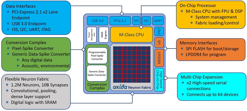
At a higher level, the Akida chip is comprised of 80 Neuromorphic Processing Units (NPU), providing 1.2 million virtual neurons and 10 billion virtual synapses. Each NPU comes with 100 KB of SRAM memory and is networked with its fellow NPUs into an on-chip mesh. Each NPU also contains eight Neural Processing Engines (NPEs) that are in charge of the convolutional support, namely matrix math, pooling, and activation. Since all of this is built around a sparse spiking-based model, the energy efficiency of these CNN operations is potentially much better than that of a GPU, CPU, or even a purpose-built AI accelerator. Levinson said the first silicon will be implemented on 28 nanometer technology and will consume between a few hundred microwatts up to a few hundred milliwatts, depending on the demands of the application.
The rest of the SoC consists of I/O and data interfaces, memory interfaces, and an Arm M-class CPU, which is only used for initial setup. There’s also an interface to create a multi-chip array of Akida devices. The compete block diagram is provided below.
Akida is not, however, suitable for training models requiring high precision. It is mainly built mainly for inference work, which is the primary use case for edge devices. That said, it will also able to do some types of incremental learning on pre-trained CNNs, a capability that separates it from competing neuromorphic designs.
So, for example, an Akida-powered smart doorbell outfitted with a camera, would be able to augment a facial recognition model to learn the faces of your family and friends, while the same device next door would be able to learn a different set of faces. That capability can be generalized across all sorts of applications where personalized unsupervised learning could be useful, like keyword spotting, gesture detection, and cybersecurity.
Although the first chip will be available as an 80-NPU SoC on 28 nanometer transistors, the platform can be delivered in various sizes and can be etched on any available process node. In fact, BrainChip will sell its technology either as SoCs or as an IP license, the latter for third-party chipmakers to integrate the neuromorphic technology into their own designs. Akida also comes with a full development environment for programmers, including the TensorFlow and Keras tools for standard CNNs, as well as a Python environment to build native SNNs.
At this point, Levinson said they are more focused on AI edge applications in industrial sensors, like smart city IoT, and similarly specialized applications that aren’t amenable to off-the-shelf solutions. While they believe the technology would be eminently suitable for smartphone AI applications, it’s a much longer-term effort to gain entrance into that particular supply chain. At the other end of the market, Levinson believes Akida also has a place in edge servers, which are increasingly being deployed in manufacturing and telco environments.
We shouldn’t have to wait too much longer to see which customer or customers take the first bite of the neuromorphic apple. The company is on the verge of taping out its chip, with shipments planned for the second quarter of the year. Stay tuned.


I’d love to get an update on how BrainChip’s IP is being used.