

Carey Kloss has been intimately involved with the rise of AI hardware over the last several years, most notably with his work building the first Nervana compute engine, which Intel captured and is rolling into two separate products: one chip for training, another for inference.
He tells The Next Platform that the real trick is to keep pace with the increasing size and complexity of training models with balanced architectures. Given that the compute required for training is doubling almost quarterly, this is more important that ever from performance, efficiency, and scalability standpoints.
Kloss and Intel think they have finally struck that golden grail of balance with the “Spring Crest” Deep Learning Accelerator, also known as the Nervana NNP-T. The name may lack the poetic ring of, say a “Volta” but we do see this training chip from its current status (they just got their first silicon back) as competitive and filling in some gaps in terms of performance/efficiency and data movement potential.
The hardware team at Intel/Nervana has taken a practical approach to building a balanced chip in conjunction with some hyperscale companies, Facebook being at the top of that list, in mind. As we discussed from OCP earlier this year, the social giant plans on giving Nvidia GPUs a run for the money in training and, we can safely assume, inference. And at our Next AI Platform event in May, head of infrastructure at Facebook, Vijay Rao, noted that they are looking forward to trying any architecture that can lend them advantage at scale for training and definitely for inference.
And finally, this week at Hot Chips, we saw a bit more about this architecture than Intel has revealed to date, including some insight into the custom network Kloss helped build for the original Nervana compute engine before the acquisition, among other elements. What strikes us about this architecture is that it is designed for scalability. And while indeed, it is possible to scale GPUs, data movement at scale has been a bit of a sticking point for large training clusters.
Nervana/Intel have the advantage of designing a training architecture from the ground up with just the workload in mind, especially at a time when most training models no longer fit on even the largest chips. This means a focus on scale-out is the only thing that makes sense, something that took some creative memory, SerDes, and other HBM tricks in addition to a robust math unit.
For nearly all models, most of the time is spent on multiply/accumulates (matrix math or convolution) which means having a lot of compute is needed (something GPUs excel at) but the massive quantity of reads coming in mean it’s possible to use one piece of data over and again, ideally reading from HBM once and using that many times with a parallel multiplier. This is a pretty standard way of thinking about the training problem. Kloss says when they dove deeper into the workloads, yes, the multipliers and SRAM and fastest HBM are critical, but the balance is harder to strike than it seems. “There needs to be enough SRAM to feed the multipliers and enough high-speed SerDes for chip-to-chip, and with HBM, everyone has the same limitations given the same HBM specs. So the trick to balance memory, on-die and off-die memory, networking, and compute.”

One of the cool features about this, and an innovation that went under the radar in most places, is that this is based on TSMC Chip on Wafer on Substrate (CoWoS) technology. It is a rather large die but definitely not huge with AI workloads in mind, at 680mm. Remember, this has no logic on the interposer, its passive, which is a smart tradeoff given design goals.
Below is the first real look we’ve had at the TPC. Keep in mind that the design goal was to spend less die area where possible including on control path logic as well as the fact that the OCP/OAM spec sizes are fixed for the foreseeable future. “We don’t want to waste die area on things we don’t need,” Kloss explains. “Our instruction set is simple; matrix multiply, linear algebra, convolutions. We don’t have registers per se, everything is a tensor (2D, 3D, or 4D).” There is a lot that is defined in software, including the ability to program the same when breaking a model to run on or off die. “Think of it as a hierarchy; you can use the same set of instructions to move data between two clusters in one group next to one HBM or between groups or even die in a network. We want to make it simple for software to manage the communication.”
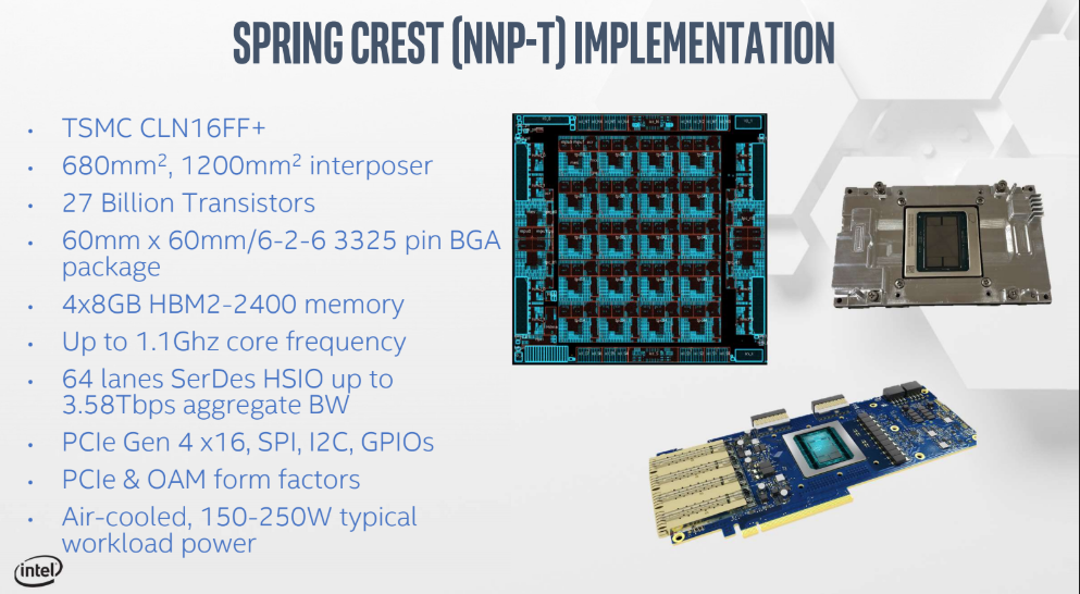
This consumes a state 150-200 Watts but when pressed about that number, we were told that was a speculative number based on part of ResNet 50, which as know, is not representative of much in the real world. We won’t see MLperf results from Intel until next year, but Kloss says they’ll have several benchmarks to show by then, including natural language processing and other workloads.
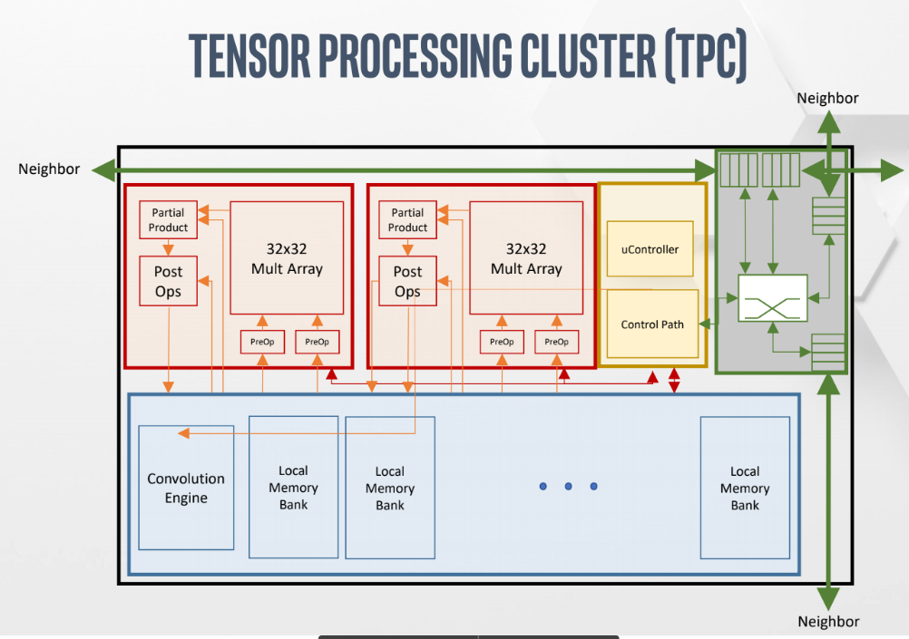
The red block is the compound math pipeline where pre- and post-operations on matrix multiply can be done with the partial products of this kept inside the multiplier array, eliminating the need for another memory port to feed partial products into the red area. That way it’s possible to get outputs on any cycle (pre-activations and post-activations) and it’s fully pipelined with both output tensors saved in the tensors.
All of what we’ve seen so far begs an important question. Other than some obvious differences in silicon, how is the math unit in this any different than say, a TensorCore inside an Nvidia Volta GPU or the TPU 3 for that matter? After all, isn’t a multiplier just a multiplier?
The answer is a bit more nuanced than it might look. As you might imagine, it goes back to tradeoffs, die area, and data movement.
“With a multiplier array like this or other competitors, you can get a lot denser with your multipliers. Once you’ve got dense multiplier arrays you’re using less die area for those multipliers and you can use your die area for more mem or other things,” Kloss says. The next decision is quantization (the quantization of the matrix multiply itself, not the weights or data). Intel chose 32×32 because when they looked at the sizes running through the neural networkss it seemed less wasteful, particularly at the boundary conditions.
“If you imagine doing a 33×33 multiply on a 32×32 array you’re going to waste a bunch of time with empty multipliers,” Kloss explains. “So if you have a much bigger multiplier array (128×128 or 256×256 as in the TPU) it’s going to scream through giant matrix multiplication but every time it hits a boundary condition it’s going to waste some multipliers–they won’t be used.” He says his team analyzed the die area tradeoffs of going bigger (64×64 up to 128×128) but since there are a just certain number of TPCs and with defined amounts of memory for they couldn’t get another row or column of TPCs with the area density savings of going that high.
“It wasn’t quite enough savings to let us have another row or column and we were limited by the die size—and this was back on Lake Crest—we were limited by how much our vendor could build. So 32×32 by process of elimination became the right tradeoff. Looking at it today it seems like a good tradeoff in terms of not wasting a lot of multipliers versus having a dense enough multiplier array.
Remember that at the beginning with the TPU, the Google team used strictly 256×256 but backed off to 128×128 in the second version after workloads changed and more real-world patterns emerged. There were two such arrays on each chip with v2 and now with v3 as we found out yesterday there are four of these per chip. Their consensus, in other words, was that 128×128 was the right answer. Volta GPUs on the other side took a different route with a 4x4x4 matrix (3D not 2D). Making comparisons at this point is still difficult, which means those MLperf training results in 2020 will be all the more interesting.
“If we look at the entrenched competition in training and die size is quite a bit bigger than our 680mm size. To get similar performance in a smaller process node with a lot less SRAM they have to have a much bigger die area. We can add more SRAM and faster networking because we are trading for a simpler instruction set. Also, assuming the OCP spec sticks, the die area will cap itself out regardless of new packaging technologies. At this point, having a more efficient use of die area will provide direct power and performance benefits.”
Also, by the way, a quick clarification point in how Intel talks about things: everything is a tensor. They don’t discuss weights, those are just considered another “tensor” but, as Kloss explains, “we do keep weights, if they’re small enough, in the SRAM. We have full control over that in software. If small enough, they can be stored in the local memory and left but if they’re bigger we can double-buffer those from the HBMs into the blue area and back out again. The multiplier arrays will just take any data from either weights or non-weights from memory banks, read them in, multiply, and spit them out again.”
There are some custom things we would expect from Nervana and Intel, including a fancy microcontroller that allows for custom instructions that handle work without complicating the precious die area. It’s possible to have several subroutines pulled out of HBM to run anything on the cluster, generating the low-level instructions to drive the SRAM and multipliers. This is handy for things like ROI pooling. In this case there is no special logic needed, just a subroutine and that creates a new instruction. This also helps on the usability side with dynamic shapes and sizes of many batches.
As another side note, it’s useful to go back in time to OCP (if you didn’t above) and check the description of the OAM mezzanine module specs and how this might fit into OCP-driven designs going forward. That really is key here and there are quite a number of useful drawings and such.
The NNP-T is in both PCIe and mezzanine form factors. Intel has been in front of the OAM mezzanine card spec with the 1.0 card in their hands soon, even with the recent spec being announced. “We like the OAM spec; it’s easier to cool and escape so many high-speed SerDes on the carrier card in the chassis,” Kloss says.
“You can see the PCIe card and two white connectors, then the four QQSFP connectors on the back of the chip: we have to do all of that to escape all the SerDes on the PCIe card, but with the mezzanine card, it’s all there and can fit into any OCP or OAM mezzanine chassis. That opens a combination of fully connected carrier cards or hybrid mesh cube carrier cards (which we prefer because it means one less link inside the chassis).” He says Intel doesn’t just want to scale these within one chassis, but go from one to another and rack to rack, hence more SerDes coming out the back of the chassis is important. “Also, our proprietary links are so fast and low latency that adding an extra hop outside the chassis doesn’t affect performance. Where others might prefer fully connected, we think it’s better to get more SerDes out of the box and go with Hybrid Mesh Cube.”
We talk more about the inference companion to the chip in a separate piece today.

What Chip Startups Can Learn from Google’s TPU Design Team
The inception of Google’s effort to build its own AI chips is quite well known by now but in the interests of review, we’ll note that as early 2013 the company envisioned machine learning could consume the majority of its compute time. Inference was a particularly expensive proposition, forcing Google …

Former Nervana Leads Target Optimal Training Configurations
Ex-Nervana Systems engineers made the jump from a hardware-centric approach to efficient training to pushing better insight into optimization of models and systems. Nervana Systems was one of the first AI chip startups to generate big buzz, culminating in an acquisition by Intel in summer, 2016. The startup’s co-founder and …
Deep Dive On Google’s Exascale TPUv4 AI Systems
It seems like we have been talking about Google’s TPUv4 machine learning accelerators for a long time, and that is because we have been. And today, at the Google Cloud Next 2022 conference, the search engine, advertising, video streaming, enterprise application, and cloud computing giant will finally make its fourth …
Be the first to comment