


With Moore’s Law running out of steam, the chip design wizards at Intel are going off the board to tackle the exascale challenge, and have dreamed up a new architecture that could in one fell swoop kill off the general purpose processor as a concept and the X86 instruction set as the foundation of modern computing.
The new architecture that they have dreamed up is called a Configurable Spatial Accelerator, but the word accelerator is a misnomer because what they have come up with is a way to build either processors or coprocessors that are really dataflow engines, not serial processors or vector coprocessors, that can work directly on the graphs that programs create before they are compiled down to CPUs in a traditional sense. The CSA approach is a bit like having a switch ASIC cross-pollenate with a math coprocessor, perhaps with an optional X86 coprocessor perhaps in the mix if it was needed for legacy support.
The concept of a dataflow engine is not new. Modern switch chips work in this manner, which is what makes them programmable to a certain extent rather than just static devices that move packets around at high speed. Many ideas that Intel has brought together in the CSA are embodied in Graphcore’s Intelligence Processing Unit, or IPU. The important thing here is that Intel is the one killing off the X86 architecture for all but the basic control of data flow and moving away from a strict von Neumann architecture for a big portion of the compute. So perhaps Configurable Spatial Architecture might have been a better name for this new computing approach, and perhaps a Xeon chip will be thought of as its coprocessor and not the other way around.
In any event, the central idea behind the CSA is easy to say, but probably hard to implement with compilers even if it does seem to open up nearly endless possibilities for a wide array of computational engines for all kinds of workloads. After the original Aurora pre-exascale machine going into Argonne National Laboratory, which Intel is the prime contractor for, was spiked last fall, we talked to Barry Davis, general manager of Intel’s enterprise and HPC group, about what technology it might use to create a machine for Argonne, and Intel was intentionally vague about it. But nothing about the CSA is inconsistent with what Davis said.
The basic idea is to take the dataflow graph of a program, which is created by all compilers, before it is crunched down to a specific processor’s instruction set and data storage and flows and lay down that data flow directly on a massively parallel series of compute elements and interconnects between them. You lay this dataflow down on static hardware etched in silicon rather than created it in Verilog or VHDL like an FPGA, so don’t be mistaken about what configurable means here.
The configurable part is that Intel will have many different CSA configurations – perhaps dozens or hundreds – tuned to the dataflows of specific applications, ranging from traditional simulation and modeling that are dominated by single precision and double precision floating point to machine learning that uses a mix of floating point and integer at various precisions, depending on if the workload is training of networks or inference classification derived from them. This is in contrast to what Intel does with its Xeon processors, which in the “Skylake” generation come in three flavors, each with 10, 18, or 28 cores and Intel turning cores and adjusting clock speeds and tweaking other features as yields and the demands for different price points dictate. With a CSA, you will want to activate as many of the underlying elements of the device as possible and not have more than you need to do any particular workload. This is not an exercise in volume manufacturing so much as mass customization for specific applications – a necessity, we think, as Moore’s Law loses power.
The CSA is being developed by Intel in conjunction with the US Department of Defense, and have come to light through a patent application filing publication that came out of the US Patent and Trademark Office back on July 5; the patent application was actually filed on December 30, 2016. Intel has filed other patents applications under this Defense Department contract, including one for scalable hierarchical interconnect topologies and another relating to symmetric addressing. The CSA patent application is interesting in that it Al Gara, the architect of the BlueGene family of parallel supercomputers at IBM as well as the architect of the Knights family of parallel processors at Intel, named on it as well as a slew of chip designers that have been working at Intel since it bought the DEC Alpha chip business so many years ago.
The CSA is also interesting in that Intel is, if the rumors are right, going to try to bring the CSA to market, first in the “Aurora” A21 supercomputer to be installed at Argonne National Laboratory, which is supposed to be the first exascale machine installed in the United States in 2021 as the name suggests. There is some chatter that the CSA could end up in other supercomputers funded by the US government with a subsequent generation of the device – the kicker to the “Frontera” machine at the Texas Advanced Computing Center that was just announced yesterday would be an obvious candidate, since it is already going to be using Intel Xeons for compute and since TACC has substantial experience with Intel’s Knights family. Frankly, after pulling the plug on Knights, Intel owes more than Argonne one. TACC is on the shortlist. But that is just a guess on our part.
The CSA approach is a minimalist one, and it puts only those computational, interconnect, switching, and storage elements onto the die that are necessary for a specific workload. The CSA starts with a grid of compute and storage elements, like this:
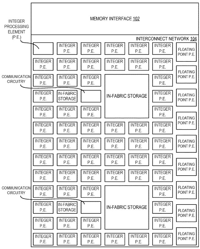
This example above has processing elements that do integer or floating point instructions as well as a grid interconnect between the processing elements and the ability to weave storage locally on the tile and linked to the fabric for the processing elements to share. This CSA accelerator could be implemented in a one-on-one fashion with cores on a Xeon die, with both having access to the same main memory, or implemented with multiple chips in a single package with an on-package interconnect, or as discrete devices with their own sockets or over the PCI-Express bus using an offload model. We suspect that Intel is not interested in an offload model, and that it will want to put CSAs in the same package as Xeons, perhaps in a many to one configuration where the Xeon is relegated to loading CSA programs and pulling data out of warm or cold storage for applications running on one or more CSAs.
This chart shows the relationship between application code, the dataflow graph created by the compiler, and the elements that are used in a CSA chip to execute that dataflow from an input to output:
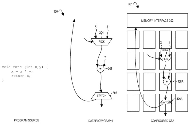
This is obviously a very simple example. The dataflows can get complex and the architecture a bit more hairy, like this:
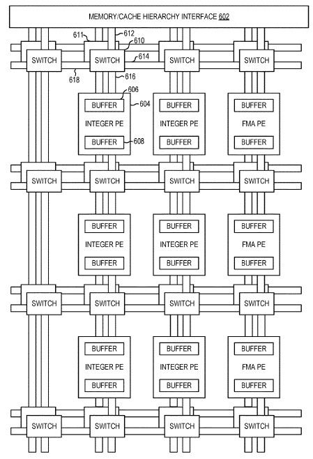
In this case, there are multiple layers of switches on the chip that interconnect processing elements that do integer and fused multiple-add (FMA) operations, and they link out to memory controllers where data is stored before it is chewed on. The processing elements have their own buffers, and the processing elements have their own registers. This can get built up further into a more complex CSA device as needed, like this:
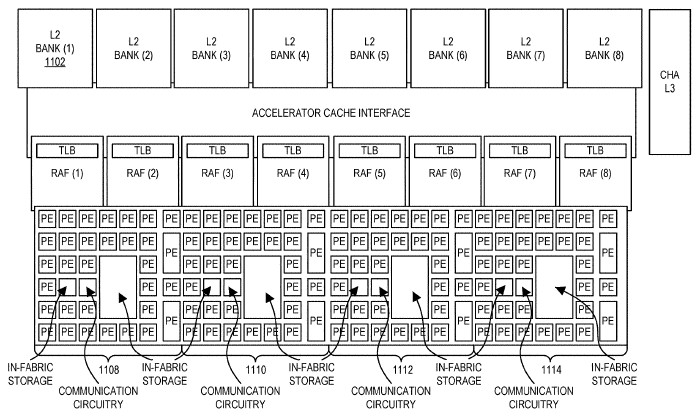
In this more sophisticated device, the clusters of processing elements are front-ended by request address files with their own table lookaside buffers, which then feed out to an L2 cache interface and L2 cache banks and perhaps a chunk of L3 cache shared by the whole shebang. The fabric on the individual CSA tiles is extended across multiple tiles and the dataflow can spread seamlessly across the elements on them as the program gets larger and the dataflow consequently gets larger. The point is, there are many ways to implement the CSA and traditional elements of CPUs can be added to the device as necessary and be completely avoided when they are not.
The main thing about the CSA approach, according to the authors, is that this presents very dense compute and memory, and also very high energy efficiency because only the elements needed for a particular dataflow are activated as a program runs. All the other stuff goes idle that is on the die. This could end up being a whole lot of dark silicon, which is wasted money, so the trick is going to be to create variants of CSA devices that are tuned to specific applications and their dataflows.
“The array of Pes may be heterogeneous, e.g, such that no PE supports the full CSA dataflow architecture and/or one or more Pes are programmed (e.g. customized) to perform only a few, but highly efficient, operations,” the authors of the patents write. “Certain embodiments herein thus yield an accelerator having an array of processing elements that is computationally dense compared to roadmap architectures and yet achieves approximately an order of magnitude gain in energy efficiency and performance relative to existing HPC offerings.” By the very nature of the devices and the dataflows they express directly from programs, the parallelism that can be exploited from programs is explicit and mapped right onto the device. The software stack for the CSA as envisioned would be able to take C, C++, and Fortran programs and directly target the CSA, like this:
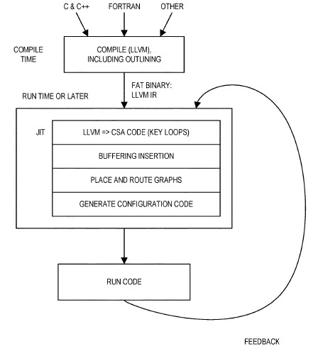
The prototype compiler that Intel is proposing for the CSA (and which we presume it has implemented if the CSA is indeed going to be used in the Aurora A21 machine) has a Clang front end that kicked out LLVM intermediate representation (IR) for the regions of code to be accelerated, and then this IR gets compiled down to the CSA itself.
Implementing legacy sequential code on this device will require come tricky interfaces to memory on the device, and Intel is obviously aware of this. The trick, says Intel, is to treat memory access as any other kind of dataflow operation.
“Embodiments of a CSA provide basic memory operations such as load, which takes an address channel and populates a response channel with the values corresponding to the addresses, and a store,” the patent application says. “Embodiments of the CSA may also provide more advanced operations such as in-memory atomics and consistency operators. These operations may have similar semantics to their von Neumann counterparts. Embodiments of a CSA may accelerate existing programs described using sequential languages such as C and Fortran. A consequence of supporting these language models is addressing program memory order, e.g., the serial ordering of memory operations typically prescribed by these languages.”
The big thing, again, is that the parallelism in the code is explicitly grabbed and mapped onto a CSA with a given configuration of processing elements, storage, switching, and such. So all kinds of parallelism – instruction, data, pipeline, vector, memory, thread, and task – can all be implemented in some fashion in a CSA device.
There is not much information in the patent application to show what the performance of a CSA might be compared to a standard Xeon CPU, but there are some hints. When the processing elements are very small compared to a CPU core (which has a lot of stuff on it to maintain state and keep data fed to the out of order execution units, and branch prediction units, and speculative execution units), the CSA approach can cram up to 16X the number of FMA units on a die as can be done with a vector processor; presumably this comparison was with the AVX-2 or AVX-512 units in the Xeons. In another citation, Intel said the floating point performance of a CSA tile could be an order of magnitude higher than a CPU core. If we are to get to exaflops within a 20 megawatt power envelope, as is desired by the HPC community, such gains will be necessary.
In its patent application, Intel showed off the CSA being implemented as a system on chip, with multiple tiles being wrapped by shared caches and memory controllers with bus controllers hanging off a ring interconnect. In another potential setup, a single CPU was linked to a CSA coprocessor with southbridge I/O controllers and main memory hanging off of the CPU as usual. Intel conceded that this could be an Arm ore MIPS processor, not just one of its own X86 devices, which was interesting. And there is another setup that shows the CSA hanging off the chipset in a two socket server like you would expect. But the next setup shows two CSAs being ganging together on a single board with point-to-point interconnects between them and the southbridge chipset for external I/O. The final image in the patent application also shows how to emulate binary code, either for an X86 chip or for another architecture, on the CSA. This is obviously easy to block diagram, but terribly difficult to do with any computational efficiency in the real world. But it may come in handy, just the same. Emulation was something that the Itanium chip did not do well, and it also had compilers that were not very good, too, and that is two reasons why it failed. So there is something to chew on.
One last thought for now, and we will be pondering the CSA quite a bit after this initial pass. Given that Intel shelled out $16.7 billion to buy FPGA maker Altera three years ago and is getting ready to ship Xeon-FPGA hybrids, what does the CSA do to Intel’s FPGA business if the CSA is easier to program and delivers better results for a lot of workloads. That is a lot of money to have spent if Intel pivots away from FPGAs and towards CSAs.