Big things can often fit into small packages, especially if those packages are tightly bound.
The concept of a specialized chiplet is as about as old as the microprocessor but due to more demands for ever more processing with power efficiency and high bandwidth the idea is being revived.
This reinvigoration of chiplets comes at a time when U.S. research arm DARPA is refreshing investment in novel architectures and approaches to processing growing data volumes. The agency’s Electronics Resurgence Initiative (ERI), is a five-year, $1.5 billion program to overcome Moore’s Law hurdles and develop new microelectronics that can fit into a wide range of government analytics and IT systems projects.
Chip giant Intel took part in the recent ERI Summit where industry and academia came together to sift through ideas for the post-Moore’s Law era of system design, including a discussion of how specialized chiplets might be the cure to some of DARPA’s woes.
The company’s director of FPGA portfolio marketing, Panch Chandrasekaran described a standard developed within the Altera group that joined Intel called the advanced interface bus (AIB) which is a die to die interconnect for connecting ever-more specialized chiplets to help organizations like DARPA quickly pull together systems based on the specialized functional building blocks.
The effort is also part of DARPA’s Common Heterogeneous Integration and Intellectual Property Reuse Strategies (CHIPS) program, which focuses on modular design and fabrication processes and the development of various, reusable IP blocks designed into physical chiplets. The goal is to create flexible systems from a catalogue of chiplets by using new and existing advanced package level integration technologies. Supporting the rapid assembly and reconfiguration of these various IP blocks, requires the establishment of standard methodologies, tools, and interfaces–both electronic and physical–that are then widely adopted by the supporting community.

Intel now provides the AIB interface license royalty-free to enable a broad ecosystem of chiplets, design methodologies or service providers, foundries, packaging, and system vendors.
“If you look at how systems are evolving, to develop anew ASIC for a specific purpose is extremely expensive with $50 million or more in development costs. This is difficult for DARPA if all they need are a few thousand components for whatever system they’re building,” Chandrasekaran explains.
“If you can build an ecosystem where it is possible to disaggregate functions into smaller building blocks it is easier to build a big library of chiplets with different functions that can be slapped together into a single package to form a system,” he adds. This is far more cost-effective, and he says with AIB, an energy efficient, open, and high bandwidth way to do so.
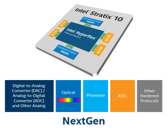
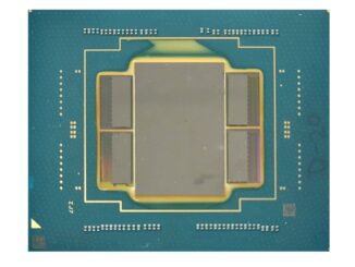
AIB has been used in Intel/Altera FPGAs including the Stratix 10 and could represent how Intel plans to handle die to die communications in its own forthcoming FPGA Xeon hybrid. This is also not limited to FPGAs; it can be used for chip to chip connectivity in a single package as long as the vendor supports the AIB.

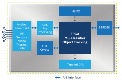
An example where this might be useful for DARPA programs is in tying together a bunch of analog sensors to an ASIC or creating a system that has a machine learning analysis component for radio frequencies or radar data. There are several components in these types of systems from the analog front end, the machine learning implementation in hardware, a processor core, and some I/O blocks. Having all of these in the form of reusable chiplets that can be tied together using AIB makes sense since IP can be repurposed easily.
AIB requests for specifications can be accessed here.


Be the first to comment