
The incumbent switch makers of the world could learn a thing or two from the server racket. Well, they actually are, but it is because the hyperscalers and cloud builders of the world have been schooling them about disaggregating the components of the switch to open up their architectures and also pushing them to make devices more programmable so they don’t have to wait years for the next chip to have what they need today.
Speaking very generally, over the past three decades that the Internet was commercialized and corporate networks shifted from a variety of different protocols and switch technologies that have gone the way of all flesh, despite the apparent openness of Ethernet and the TCP/IP protocol stack that is the backbone of the Internet, switch chip and switch makers alike have been extremely secretive about the components inside of their switches. They loved the control – physical and psychological and technical and economic – that the appliance model brought them over those decades.
We find this annoying, and celebrate those merchant switch chip makers – Broadcom, Mellanox Technologies, Barefoot Networks, Cavium, and Innovium are the big ones in the datacenter – that talk about their technology in detail. It still is nowhere as deep a dive as we get from the CPU makers of the world, and the elements of the switch are nowhere as close to being itemized as we can do on any server that any OEM or ODM wants to put together. Someday, perhaps.
Recently, we were particularly irked during the Cisco Live extravaganza put together by datacenter switching juggernaut Cisco Systems to find out that the company had, in fact, adopted the “Tofino” programmable switches from Barefoot Networks, but decided that it didn’t want to confirm this fact much less actually talk about its plans for programmable switches and its desires to make inroads back into the hyperscaler and cloud builder datacenters or make programmability something that is approachable for the very large customer base that the company has in the enterprise. Cisco doesn’t really have any presence in HPC, excepting that among some financial services companies that have distributed fraud detection and risk analysis clusters and have a penchant for buying Cisco switches because of their familiarity with either the iOS or NX-OS switch operating systems.
The intimate knowledge that network admins have with these Cisco switch operating systems, paired with different switch ASICs, either homegrown or bought from merchant silicon suppliers, is why Cisco still commands dominant share of the datacenter switching market. But that share has fallen from a very steady 65 percent through the Internet boom down to around 50 percent – and there are reasons for that. The main one is that upstart switch makers have adopted upstart merchant silicon, and they have changed the competitive landscape, pricing, and pace of innovation in the market. And rather than fight them, Cisco has been forced to join them. Even if it doesn’t really talk about it. At least not loudly.
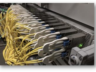
We poked around a bit, and have found this beautiful presentation that Cisco technical marketing engineer Faraz Taifeshesmatian gave at Cisco Live, detailing the merchant silicon in use in the Nexus 3000 line of top of rack switches that the company sells against the whitebox makers as well as Arista Networks, Juniper Networks, Mellanox, Dell, and Hewlett Packard Enterprise in the Ethernet space. It details everything, and it shows the kind of openness that we advocate. We were unable to attend Cisco Live, but this is one that we would have wanted to sit in on. Taifeshesmatian did not talk about the Nexus 9000 chips, which have Cisco’s homegrown “Alpine” and “Northstar” ASICs and which have its Application Centric Infrastructure (ACI) software-defined networking extensions baked in, and he did not talk in detail about the merchant silicon chips used in the Nexus 9200, 9300, and 9500 switches, either. But the chart below does mention them:
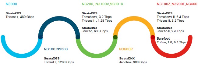
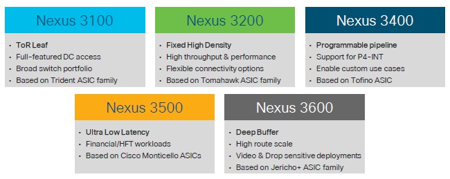
As you can see, Cisco has adopted a wide variety of chips from Broadcom – the Trident, Tomahawk, and Jericho families – over the past few years, and just recently, with the Nexus 3400, has adopted the Tofino chips from Barefoot Networks. This chart below sums up the target markets and feature sets for the various Nexus 3000 switches:
Here is the wonderful thing about this presentation that Taifeshesmatian put together. It actually gives some of the technical details of the chips that Broadcom and Barefoot themselves do not reveal. (A heartfelt thank you for that.)
Let’s take them in order, starting with the Nexus 3000 family. The Nexus 3100 was based on Broadcom’s “Trident-2” ASICs, which delivered 1.28 Tb/sec of aggregate bandwidth and had a 12.2 MB buffer. With the Nexus 3100-V, Cisco moved on up to the “Trident-2+” ASIC, which boosted the buffer to 16 MB and had the same bandwidth. The Nexus 3100-Z adopted the “Trident-3” chip from Broadcom, which boosted the bandwidth by 2.5X to 3.2 Tb/sec and the buffer by 2X to 32 MB.
Here is the pretty block diagram of the Trident-3 chip:
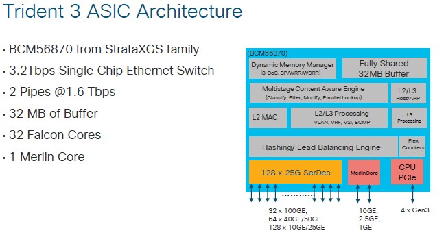
There is a “Falcon” core for each one of the 32 ports running at 100 Gb/sec in this 1U switch, plus a single “Merlin” core running at 10 Gb/sec for management purposes. The Trident-3 chip has two packet processing pipelines, each with sixteen of the Falcon cores, and these are cut into two into two groups of Falcon SerDes. Each quarter of the SerDes blocks has access to one quarter of the forwarding bandwidth of the ASIC.
This is how the Trident-3 is actually implemented in the Nexus 3100-Z switch:
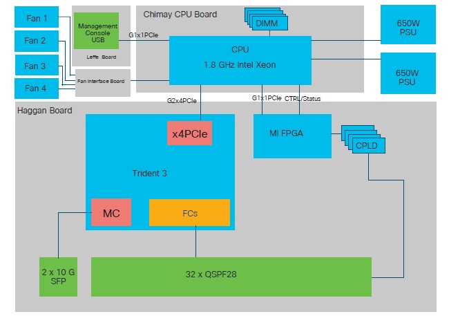
As you can see, this switch is a hybrid server in its own right, with not only the Trident-3 ASIC, but a 1.8 GHz Xeon processor with its own memory (our guess is that it is a Xeon-D chip from Intel) on a board code-named “Chimay,” plus an FPGA and a series of complex programmable logic devices (CPLDs) sitting between the ports and the FPGAs to accelerate certain functions outside the loop of that switch chip. The Xeon processor is linked to the switch ASIC and to the FPGA over PCI-Express links.
Moving on up to the Nexus 3200, the original machine was based on the “Tomahawk-2” ASIC from Broadcom, which had 3.2 Tb/sec of aggregate switching bandwidth and which had four blocks of 4 MB of buffer memory for a total of 16 MB. The new Nexus 3200-E switch is also based on a rev of the Tomahawk-2, but it is one rated at 6.4 Tb/sec and with four blocks of 10.5 MB of buffer memory for a total of 42 MB.
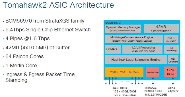
This Nexus 3200-E basically doubles up a lot of stuff, with 6.4 Tb/sec across four 1.6 Tb/sec pipelines based on 64 Falcon cores for 64 ports running at 100 Gb/sec and one Merlin core for management that can run at 100 Gb/sec. These ports can all be split into multiple slower ports, as shown in the block diagram.
Here’s the architecture of the Nexus 3200-E switch:
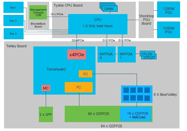
There is a different compute board back there, called the “Tyskie,” that still has a 1.8 GHz Xeon CPU with memory slots of its own. This might be an updated Xeon-D chip. The Nexus 3200-E has a block of 48 Falcon cores doing regular 100 Gb/sec ports, and a block of 16 ports that have MACsec encryption added to the ports for encrypting data on the fly as it comes in and out of the switch. This chip also has two FPGAs for function acceleration.
It is interesting that Cisco has not yet announced a switch based on the “Tomahawk-3” chip from Broadcom, which was announced in January, but we suspect it will come out by the end of this year or early next year.
Now we can move on up to the Nexus 3400. This is the new switch that is based on the Tofino programmable chip from Barefoot Networks. Cisco is announcing a Tofino switch in the 3400 line with 18 ports running at 100 Gb/sec using the 1.8 Tb/sec entry Tofino ASIC, but it also shows that it has adopted the high-end 6.4 Tb/sec part, which means there is a 64 port Nexus 3000 series switch in the works.
This is a fairly modest implementation of the Barefoot family:
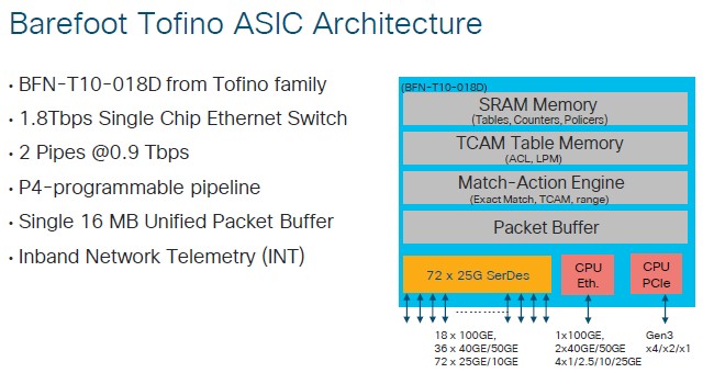
The ports can be broken down to run at 36 ports running at either 40 Gb/sec or 50 Gb/sec or 72 ports running at 10 Gb/sec or 25 Gb/sec, which is important to some service providers, hyperscalers, and cloud builders. There is a single 100 Gb/sec management port, of course, on the Tofino chip, and it can be chopped up as needed. The chip is carved up into two blocks running at 900 Gb/sec, with a single 16 MB unified packet buffer and, of course, a pipeline that is entirely programmable in the P4 language that Barefoot Networks has created and open sourced.
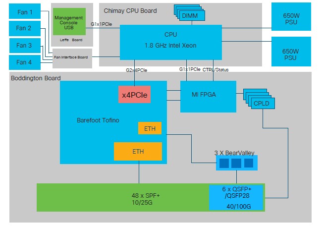
The Nexus 3400 looks a lot like the Nexus 3100, with some of the “Bear Valley” MACsec encryption circuits added on some of the ports like in the Nexus 3200. In fact, it looks pretty much like an ASIC swap with a slightly different port configuration. Take a look:
Now we can move up to the Nexus 3500, which has been in the field for six years now and which is based on Cisco’s own “Monticello” ASIC. This Nexus 3500 box is aimed at high frequency trading applications, and while it only has 10 Gb/sec ports, the latency on a port to port hop is as low as 250 nanoseconds, which is quite a bit lower than the typical 450 nanoseconds of a relatively fast Ethernet switch.
Here is the block diagram of the Monticello ASIC:
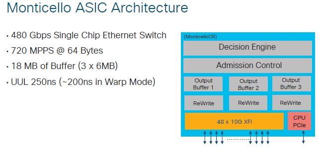
The Monticello chip has three blocks of buffers delivering its 18 MB of capacity, and the packet forwarding engine can deliver 480 Gb/sec of aggregate bandwidth and process 720 million packets per second. Again, this is no great shakes but the latency – and consistent latency – is what matters.
Here is the block diagram of the Nexus 3548 switch:
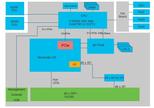
This switch is really showing its age a bit, but it is still probably widely used in the financial services industry. The Nexus 3548, which is the only instantiation of the Nexus 3500, has a two core “Ivy Bridge” Core i3-3227U processor from Intel that is overclocked to 2.5 GHz from its rated speed of 1.9 GHz. This processor has 16 MB of its own flash to boot from plus DRAM memory. The Nexus 3548 has an FPGA in the box and can support 48 ports running at either 10 Gb/sec or 25 Gb/sec – that last bit is neat because the 25G standard was not announced until years after the 25G Ethernet standard was put out. So clearly, there is some software-defined functionality and golden screwdriver going on with the Monticello ASIC. Which is fine.
And last but not least, there is the Nexus 3600 line of deep buffer switches, which are based on Broadcom’s “Jericho+” ASICs. The initial Nexus 3600 had a pair of Jericho+ ASICs to deliver 1.8 Tb/sec of switching bandwidth and had 8 GB (that’s gigabytes not megabytes) of buffer capacity, and the second generation, which is new this year, has four Jericho+ chips to double that all up to 3.6 Tb/sec of switching bandwidth and 16 GB of buffer capacity.
Here’s the Broadcom Jericho ASIC block diagram:
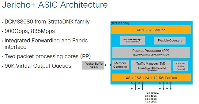
Each Jericho+ chip can do 900 Gb/sec of bandwidth and handle 835 million packets per second, and the chip has a pair of packet processing cores with 96 virtual output queues. Those packet buffers are based on the same GDDR5 memory that is used in graphics cards.
Here is the architectural layout of the latest Nexus 3636 switch:
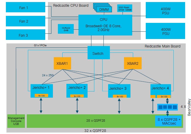
The processor board on this switch is called “Redcastle” and it is based on an eight-core “Broadwell” Xeon-D chip that runs at 2 GHz. The server board embedded in the switch has 2 MB of NVRAM memory sitting beside its DRAM main memory, plus a 128 GB flash drive for booting up the NX-OS network operating system. There is a PCI-Express switch linking the CPU complex to the four Jericho chips, which have their own crossbar circuits for linking to each other. (This is in essence a two-tier network in a box acting like a single switch.) The Nexus 3636 switch has four of the Bear Valley chips on the board, which provide MACsec encryption on eight of the 32 ports in the box.
Now we know.

Is AWS Making The Switch To Homegrown Network ASICs?
Amazon Web Services, the juggernaut of cloud computing, may be forging its own path with Arm-based CPUs and associated DPUs thanks to its 2015 acquisition of Annapurna Labs for $350 million. But for the foreseeable future, it will have to offer X86 processors, probably from both Intel and AMD, because …

Billion-Dollar AI Promise a Bright Spot in Gloomy Quarter for Cisco
Cisco navigated a rocky road in its first quarter of the year as evidenced by the dips in share price for the networking giant this morning. However, like its other public tech peers, Cisco is pointing to AI as the savior of all systems spending, claiming $1 billion in AI-centric …
Why Not Networking As A Service? But How?
In 2019, Hewlett Packard Enterprise was the first top-tier tech vendor to make the plunge, announcing that it planned to make its entire portfolio – all of its hardware as well as software – available as a service by 2022, leveraging its GreenLake hybrid cloud platform to answer the call …
Be the first to comment