

In the long run, networking chip giant and one-time server chip wannabe Broadcom might regret selling off its “Vulcan” 64-bit Arm chip business to Cavium, soon to be part of Marvell. The ThunderX2 processors based on the Vulcan designs have been tweaked by Cavium and have been enthusiastically tire-kicked by hyperscalers and HPC centers alike, and are looking like the front runner as a competitor to the X86 architecture for these customers.
The 32-core Vulcan variants of the ThunderX2, which we detailed last November, are getting their own coming out party in San Francisco now that they are generally available. Many of the technical details that have been shrouded until now and some pricing for the chips are being revealed today, so let the comparisons begin. The Vulcan ThunderX2s will be eventually joined by the 54-core ThunderX2 chips (we don’t know their code-name) that Cavium itself designed, which sacrifice some memory bandwidth to boost compute throughput and are aimed at more generic cloud and hyperscale workloads and not so much at hyperscale and HPC jobs that are bound when it comes to memory capacity and bandwidth. This ThunderX2 variant will be positioned more against the Qualcomm “Amberwing” Centriq 2400 chips, also based on a homegrown 64-bit Arm core and also trying to take a bite out of Intel’s “Skylake” Xeon SP line and keep AMD’s “Naples” Epyc X86 chips from making too many inroads into the datacenter as the Xeon alternative. Cavium will also face some competition from Ampere, the startup that bought and is set to relaunch the X-Gene product line from Applied Micro, and from IBM with its “Nimbus” variant of the Power9 processor.
It is a good time to be a CPU shopper, that’s for sure. We have not seen this level of competition in two decades. And Intel is probably wishing it had crammed eight memory controllers on the Skylake die, too, and not left itself open to this competition. But here’s the funny thing. There is apparently enough growth in the server market to accommodate many architectures, and Intel’s numbers in the first quarter have not been hurt one bit by the competition with Arm, Epyc, and Power. One little recession and this could get real interesting, real fast. . . .
The Feeds And Speeds
We knew a bunch of things about the Vulcan variants of the ThunderX2, which was revealed by Cavium last fall, but the company was holding back a bunch technical details until the official launch of the chip. We will start from the outside and work in.
Here is the latest-greatest system-on-chip block diagram for the Vulcan ThunderX2:
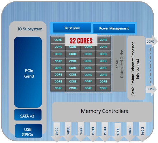
The chip has 32 cores, which have a custom design with out of order execution and simultaneous multithreading (SMT) to boost the performance. The out of order circuits are quad issue, and fully out of order, which is common in RISC processors dating back to the 1990s. The cores are based on the Arm v8.1 specification and are modified from there; they are designed to scale up to 2.5 GHz and are etched in the 16 nanometer processes from Taiwan Semiconductor Manufacturing Corp.
Last November, when the Vulcan chips were unveiled, Cavium had planned to sell variants with 24, 28, or 32 cores to match meet or beat the core counts in the very top bin Skylake Xeon parts, but Gopal Hegde, vice president and general manager of the datacenter processor group at Cavium, tells The Next Platform that based on customer demand, the company has widened out the SKU stack to over 40 different variations, and it is offering chips with 16, 20, or 30 cores as well; clock speeds range from lows of 1.8 GHz to 1.6 GHz, which were requested by customers using the chip for software-defined storage applications, to a high of 2.4 GHz to 2.5 GHz, which are pushing the envelope on the TSMC processes and the overall performance of the Vulcan chips. (The original Vulcan plan at Broadcom, which we revealed here, was to push the clock speed up to 3 GHz on this 16 nanometer process. We don’t know if these Vulcans topped out at 32 cores, however. We suspect that was the plan all along.
The Vulcan cores all support turbo boosting, provided the chip stays within its thermal envelope so it doesn’t let out the magic blue smoke that makes all processors work. There are two turbo modes: one when just a single core is running and one when all of the cores are running, and the peak speed with just one core is 2.96 GHz. The turbo with all cores activated will depend, but our guess is it is something around 100 MHz to 300 MHz across a wide range of active cores and workloads.
The new bits of data about the Vulcan ThunderX2 cores include the fact that the Vulcan chips will support SMT modes with 1, 2, or 4 threads active per core, and Hegde says that the two-thread SMT boosts throughput by about 20 percent and the four-thread SMT pushes it up by around 30 percent. That’s about as good as Intel gets with two-thread HyperThreading on its Xeons and about as good as IBM gets on four-thread SMT on the Power8 and Power9 chips, although IBM can push it up to eight threads per core if customers want to do that on the Power8 chips and certain models of the Power9 chips and get more oomph for workloads that are amenable to lots of threading – think web application servers, Java and PHP runtimes, and databases.
We have also learned that the Vulcan cores sport two 128-bit NEON floating point units, which gives it the ability to chew through 256 bits of floating point math each clock cycle per core. This half the oomph of the pair of AVX2 math units in the “Haswell” and “Broadwell” Xeon E5 cores, which could do 32 single precision or 16 double precision floating point operations per clock. Intel has, of course, moved on to AVX-512 in the Skylake Xeons, which have 512 bits and which can do twice that or 64 single precision or 32 double precision flops per clock.
We expected that the Vulcan chips would have up to eight DDR4 memory controllers, but we did not know that they could support DDR4 memory speeds up to 2.67 GHz. The chip can have one or two DIMMs per channel, or eight or sixteen memory sticks per socket. Cavium is supporting RDIMM, LRDIMM, and NVDIMM-N memory (the latter available from Hynix and used by some hyperscalers for capacitor-backed main memory) in the system. Single, dual, and quad ranked memory modules are supported, with up to 32 memory slots on a two-socket system. Our guess is that you have to run slower memory if it is fatter, which is standard practice in servers. Cavium is claiming that it has 33 percent memory capacity and 33 percent memory bandwidth advantages over the Intel Xeon SP chips. (We will be diving into the performance comparisons between the Vulcan ThunderX2 and Xeon processors in a separate story.)
The Vulcan ThunderX2 also has a bunch of reliability features on the memory to make it server class, including 1-bit error correction and 2-bit error detection, memory address parity protection, demand and patrol scrubbing, failed DIMM identification, and error containment for data poisoning. (Here at The Next Platform, we get data poisoning all the time.)
The Vulcan chip includes a second generation NUMA chipset, called the Cavium Coherent Processor Interconnect (CCPI2), which runs at 600 Gb/sec and which currently scales to two socket implementations. But we figure this NUMA interconnect can be pushed to four sockets if need be. This CCPI2 interconnect is implemented with 24 SerDes running at 25 Gb/sec bi-directionally, and is functionally similar to the NVLink ports on “Pascal” and “Volta” GPU accelerators from Nvidia and on Power9 chips from IBM as well as the “Bluelink” OpenCAPI ports on the Power9 chips. It would be very interesting to see these SerDes tweaked to speak OpenCAPI or NVLink.
On the peripheral I/O front, the Vulcan chip includes fourteen PCI-Express 3.0 controllers – a new fact – that delivers up to 56 lanes of I/O across the socket. The SoC also includes a SATA v3 peripheral controller, USB3 peripheral controllers, and various general purpose I/O ports. Trust Zone encryption coprocessors and power management controllers are also embedded on the SoC, and there is no additional chipset required to use it in either a one socket or two socket configuration. (This is not true of the Xeon chips, importantly.) The chips come in LGA sockets as traditional server manufacturers like (and allow for a Xeon socket to be swapped out of a motherboard and a ThunderX2 to be mapped in relatively easily) and also have a directly soldered BGA option that Hegde says is popular with the hyperscalers and cloud builders who are minimizing manufacturing complexity. That last bit is new data, too.
This block diagram of the internal architecture of the Vulcan chip is also bright and shiny:

The Vulcan chip is fully virtualized, as you might expect this being a necessary thing for the foreseeable future, supporting the SMMUv3 memory management and GICv3 generic I/O management specifications from Arm Holdings.
As you can see, the heart of the design is a ring interconnect, which Hegde says has an aggregate of 6 Tb/sec of bandwidth across this fabric, which is completely non-blocking. That means that any core can access any information in any other core and any core can access any memory controller and reach into main memory, and do so without oversubscription over the bi-directional ring. (This is a very similar approach to what Intel did with the past several generations of the Xeon, until it moved to a mesh networking with the three different Skylake Xeon chips.)
Up until now, we did not officially know much about the cache hierarchy in the Vulcan chips, but now we can finally see it. (We did dig around and find the old Vulcan presentations that Broadcom was making and had many of these details, which we told you about last fall. But they could have changed.)
Each core has 32 KB of L1 data cache and 32 KB of L1 instruction cache, and another 256 KB of L2 cache. The cores are organized into blocks of four, and each block as a port on that coherent ring interconnect and access to two slices of 2 MB of L3 cache eight there on the ring, for a total of 4 MB per block of four. Across eight of the four-core blocks, there is a total of 32 MB of distributed and shared L3 cache, which is a ratio of 1 MB per core. That’s not too shabby, but it is nowhere as big as what Intel does in the Xeons. (Intel has been cache heavy, particularly back in the days of the front side bus.) The ring, as you can see, has a port for hooking out to the CCPI2 interconnect, and two ports linking out to the DDR4 memory controllers – one right and one left, each with four controllers on it. There is another port that links out to a non-coherent I/O interconnect bus, which is where all of the I/O controllers and those PCI-Express 3.0 controllers all hang off of. The wonder is that Cavium did not update these to PCI-Express 4.0, but that would have taken time and money and perhaps for little gain given that only the Power9 chip supports PCI-Express 4.0 at the moment.
That brings us to the actual Vulcan ThunderX2 SKUs that are being sold, so without further ado, here they are:
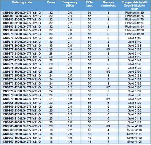
There are only 35 SKUs in that table, so there must be at least six custom parts that Cavium is making, and possibly more, to get more than 40 variations as Hegde confirmed to us.
The top-end 32 core chip running at 2.5 GHz will sell for under $3,000 each in 1,000 unit trays, and it tops out at 200 watts. Hegde says that the 2.2 GHz chip with 32 cores will be the mainstream high-end chip that sells, and it will come in at 180 watts and cost only $1,795. The low-end 16 core chip running at 1.6 GHz has a 75 watt thermal envelope and costs a mere $800. Speaking very generally, the low-end SKUs with lower clocks and fewer cores are aimed at storage workloads, the top bin parts are aimed at hyperscalers and cloud builders running their own applications and maybe selling capacity to the public as well as very high end HPC shops. The midrange parts are aimed at second-tier cloud builders who are more budget conscious as well as HPC shops that have to balance cost, thermals, and performance against each other in slightly different ways. The ten SKUs that Cavium expects to be its volume parts are:
- 32 core, 2.2 GHz
- 32 core, 2.1 GHz
- 32 core, 2 GHz
- 30 core, 2.2 GHz
- 28 core, 2.2 GHz
- 28 core, 2 GHz
- 24 core, 2.2 GHz
- 24 core, 1.8 GHz (the power optimized SKU)
- 20 core, 1.8 GHz
- 16 core, 1.8 GHz
The Vulcan ThunderX2 processors are available now, in volume. Next up, we will try to get a handle on the performance, performance per dollar, and performance per watt of these processors and how they stack up to the Xeon SP chips first and then other alternatives. There is a lot to consider here.

One On One With Jensen Huang: Nvidia, The Platform Company
While a lot of ideas are ancient, some are relatively new and can come from only a modern context. Platform is one such concept, and given what we care about here at The Next Platform, it bears some analysis as we consider the company the Jensen Huang, co-founder and chief …

Talking Chip With Ampere Computing CEO Renee James
Outside of the HPC market where there are a number of companies that have delivered or are working on Arm-based server processors, Ampere Computing is the main independent supplier of Arm-based server chips with its current 80-core Altra chips and its impending 128-core Altra Max chips, which are sampling now …
Alibaba Rumored To Enter The Arm Server Chip Race
The chip cold war between China and the United States continues to heat up like a processor with a heat sink that it is a little too small. And the scuttlebutt is that this week Alibaba, the Chinese online retailer and cloud service provider that is roughly analogous to Amazon …
“Vulcan cores sport two 128-bit NEON floating point units, which gives it the ability to chew through 256 bits of floating point math each clock cycle per core. This is akin to the same level of raw performance that the AVX2 math unit in the “Haswell” and “Broadwell” Xeon E5 processors, which could do 32 single precision or 16 double precision floating point operations per clock. Intel has, of course, moved on to AVX-512 in the Skylake Xeons, which have 512 bits and which can do twice that or 64 single precision or 32 double precision flops per clock.”
This sounds a bit off. Two 128-bit units with FMA give 16 SP / 8 DP operations per clock. So Haswell and Broadwell have twice the FPU throughput. Which is to be expected since they have two 256 units!
Also, IIRC some CPUs (Bronze, Silver and even some Gold SKUs) that support AVX-512 do not have the dedicated AVX-512 unit enabled. So they fuse the two 256 units into one which yields the same throughput as HW/BW. Of course, when the dedicated AVX-512 unit is enabled that doubles the ops per clock. But at the expense of lower clocks.
Hitachi has announced plans to implement arm Scalable Vector Extensions. This would put arithmetic performance at least on par with xeon, probably beyond. Without that, it’s hard to justify the jump to arm. Compared to skylake, the vulcan TX2 has better memory bandwidth but fewer flops, and only slightly lower cost. Compared to AMD, it has the same bandwidth, similar flops, and similar cost, but you have to recompile your software. Arm is clearly the best non-x86 architecture for HPC, but second place is a long way short of first.
Where are the SPEC CPU2017 rates for any of those ThunderX2 CPUs?
– Let me ask a question with regard to the comment for the pricing:
– “The top-end 32 core chip running at 2.5 GHz will sell for under $3,000 each in 1,000 unit trays, and it tops out at 200 watts. Hegde says that the 2.2 GHz chip with 32 cores will be the mainstream high-end chip that sells, and it will come in at 180 watts and cost only $1,795. The low-end 16 core chip running at 1.6 GHz has a 75 watt thermal envelope and costs a mere $800.”
– Top end 32C/2.5GHz’s pricing $3,000 is a lot competitive than Intel Platinum 8180($10,009 at Intel hompage) -> 30.0%
– Main Stream 32C/2.2GHz’s pricing $1,795 is also competitive than Intel Platinum 8164’s $6,114. -> 29.4%
– However, lowend’s one is quite strange. 16C/1.6GHz’s $800 is quite higher than Intel Silver 4108’s $417. -> 191.8%.
– It would be much appreciated if we can get a double confirm on this. I made SKU comparison with the table on this article.